Introduction to RF Power Measurements
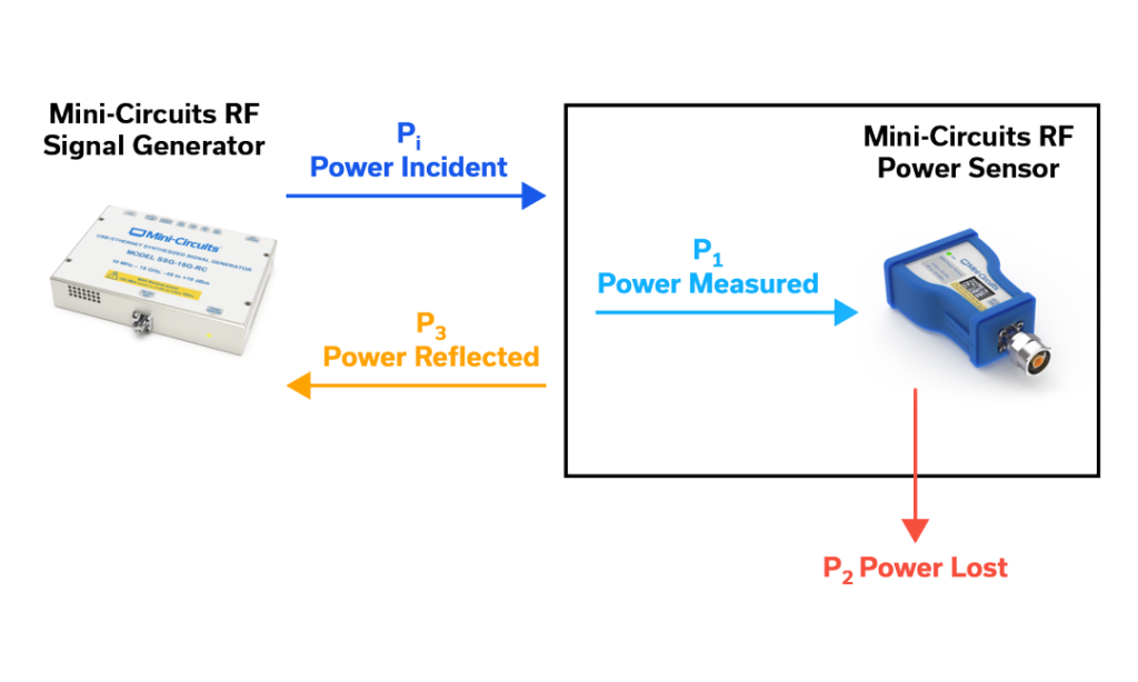
Power is a necessary parameter to measure across a wide range of modern applications. Power is defined as work per unit of time. It includes units of measure such as horsepower, watts, calories per second and BTU per second, depending on the domain of interest. Electrical power is typically measured in watts, defined as one Joule per second. With RF circuits, dBm, a logarithmic representation of power level relative to the milliwatt, is often used.
An assortment of instruments and methods are used for measuring power. In this article, we will limit the discussion to electrical power, defined as voltage multiplied by current. We will further narrow the discussion to RF power, which implies higher frequency, say signals greater than 10 MHz, requiring more sophisticated instrumentation than a voltmeter due to the behavior of high-frequency electrical signals.
It is important to select the appropriate technique for measuring RF power in a given scenario. If the signal level is too high, the instrument input will become saturated; distortion, harmonics, spurious and other non-linear signals could occur. If the signal level is too low, the signal will be buried in the noise floor, making it difficult to retrieve.
Group Delay in RF Filters
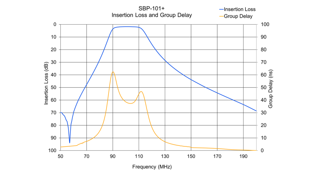
The concept of group delay as it pertains to RLC networks was first described by Harry Nyquist in 1928.1 The contributions Nyquist made to the field of Communications Theory are well known,2 and still applicable to modern day communications systems. On our way toward understanding group delay in this brief application note, we’ll start by examining phase delay. After mathematically defining phase delay, we will then continue by defining group delay. Illustrations of amplitude response, and phase and group delay response for several ideal filters of various filter topologies are shown. This app note concludes with a display of magnitude and group delay frequency response curves for two real filters designed and manufactured by Mini-Circuits, both of which have the same filter topology.
Selecting VCOs for Clock Timing Circuits – A System Perspective
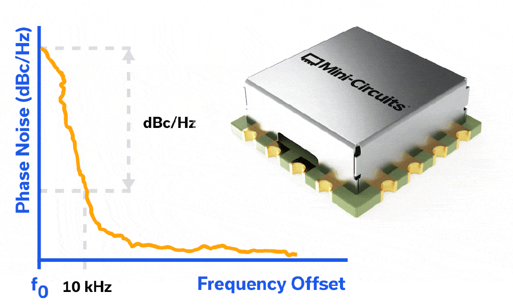
Timing is critical in digital systems, especially in electronic systems that feature high-speed data converters and high-resolution sampling. A clock source is the “timekeeper” and the system performance depends upon the effectiveness of this component. For some system designers, implementing a clock source automatically means using a crystal oscillator, typically a single-frequency source. But other designers, especially those tasked with synchronizing systems at multiple clock frequencies, have learned to appreciate the flexibility of using voltage-controlled oscillators (VCOs) as clock sources.
Fast-Switching GaAs Switches Are a High-Performance, Low-Cost Alternative to SOI
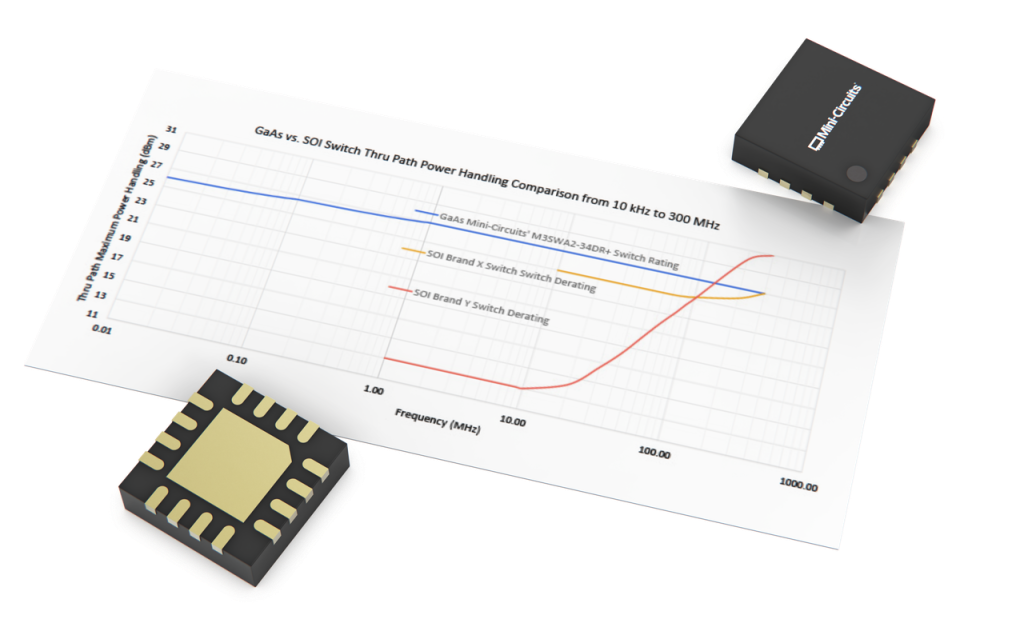
A mistaken belief has arisen in recent years that SOI has somehow taken over as the prevailing technology for fast RF switch applications, but not so fast! Mini-Circuits’ recent introduction of the M3SWA2-63DRC+ and the M3SWA2-34DR+ ultrafast, absorptive RF switches has given cause for designers to reconsider their switch choices. Designers are discovering that it is no longer necessary to bear the expense of an SOI switch just to get the speed they need.
In this application note, we perform a comprehensive, side-by-side, parametric comparison of the Mini-Circuits’ wideband GaAs MMIC M3SWA2-34DR+ switch to two SOI competitive offerings. This comparison leads us to the conclusion that there is no reason to take your foot off the GaAs.
Measurement of Amplifier Additive Phase Modulation Noise (APM)
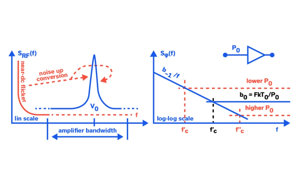
In our efforts to properly characterize the Additive Phase Modulation Noise (APM) and Additive Amplitude Modulation Noise (AAM) performance of MMIC amplifiers in our labs, Mini-Circuits is careful to consider the performance capabilities and limitations of our phase noise analyzer and test setup (see Figure 4). Both APM and AAM performance can be dependent upon the analyzer’s internal signal source carrier frequency, power level, and, importantly, the phase length from signal source output to RF input, so great care must be taken to optimize these parameters.
Frequency Modulation Fundamentals
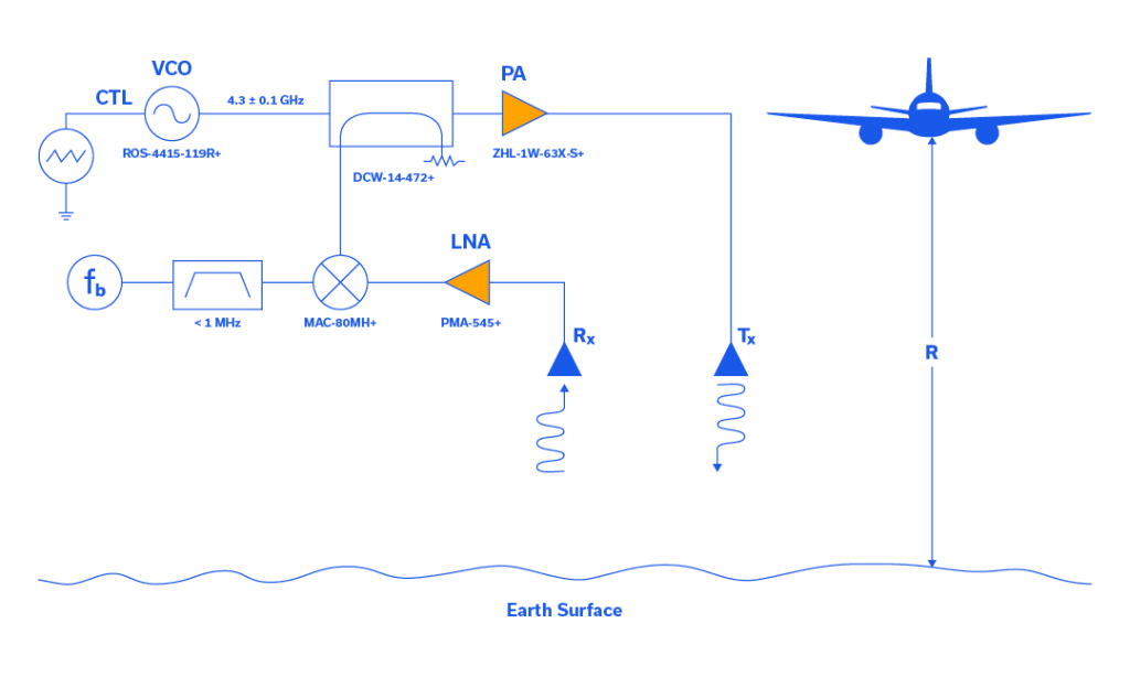
In the 1920s, many brilliant scientists applied themselves to the study of frequency modulation (FM). One of these scientists was a communications systems theorist who worked for AT&T named John Renshaw Carson. Carson performed a comprehensive analysis of FM in his 1922 paper which yielded the Carson bandwidth rule.1 Carson was so convinced that FM was not a suitable solution to the static found in AM transmission systems that he once remarked, “Static, like the poor, will always be with us.”2
Beginning in 1923, in Columbia University’s Marcellus Hartley Research Laboratory, in the basement of Philosophy Hall, a driven genius in electronic circuitry named Edwin Howard Armstrong set out to reduce static through the use of FM. After approximately 8 years of toil, Armstrong had a brainstorm and decided to challenge the assumption that the FM transmission bandwidth had to be narrow to keep noise low. After painstakingly designing this new FM system, with as many as 100 tubes spread over several tables in the laboratory, “[Armstrong] was able to prove that wideband FM made possible a drastic reduction of noise and static.”3 Armstrong was issued patent number US1941069A, which specifically addresses noise suppression in wideband FM, on December 26, 1933, along with three additional patents for FM that same day.
The Basics of Orthogonal Frequency-Division Multiplexing (OFDM)
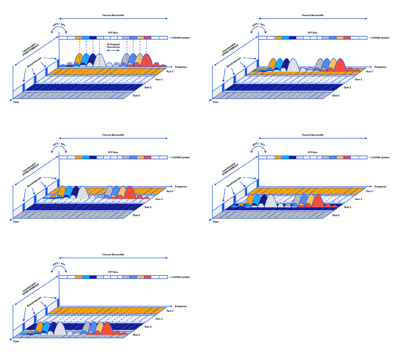
While traditional Frequency Division Multiplexing has been around for over 100 years, Orthogonal Frequency Division Multiplexing (OFDM) was first introduced by Robert W. Chang of Bell Laboratories in 1966.1,2,3,4 In OFDM, the stream of information is split between many closely-spaced, narrowband subcarriers instead of being relegated to a single wideband channel frequency.5 Single-channel modulation schemes tend to be sequential whereas, in OFDM, many bits can be sent in parallel, simultaneously, in the many subcarriers.5 So many bits can be packed onto the subcarriers simultaneously that the data rate of each subcarrier’s modulation can be much lower than that of a single-carrier architecture.
LTCC High Pass Filters for mmWave
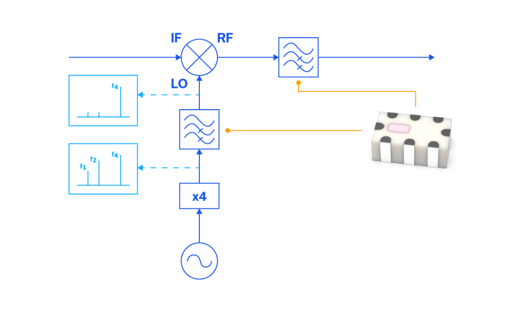
Mini-Circuits has introduced new high pass filters that achieve breakthrough performance for Q-band and lower V-band applications up to 58 GHz. The HFCQ, HFCN, and HFCV LTCC filters offer a combination of low insertion loss, high return loss, excellent rejection, small size, cost-effectiveness, repeatability, ruggedness and reliability. These filters enable designers to cover filter blocks with traditional SMT technology versus more exotic solutions. Key benefits include smaller footprint compared to stripline filters, repeatable performance suited for volume production, and robustness. The filters simplify designs for applications like 5G FR2 and satellite communications. Mini-Circuits’ latest LTCC high pass filters set a new standard for electrical performance and ease of implementation in demanding mmWave systems.
MMIC Package Customization – Footprint-Compatible Solutions for Your System
MMIC Package Customization – Footprint-Compatible Solutions for Your System Obsolescence Management and EOL Part Replacement LTB (Last Time Buy) and EOL (End of Life) are among the most unwelcome acronyms in the ranks of Procurement and Engineering. Component obsolescence saddles customers with the burden of tying cash up in inventory on their balance sheet, or […]
MIMO Systems
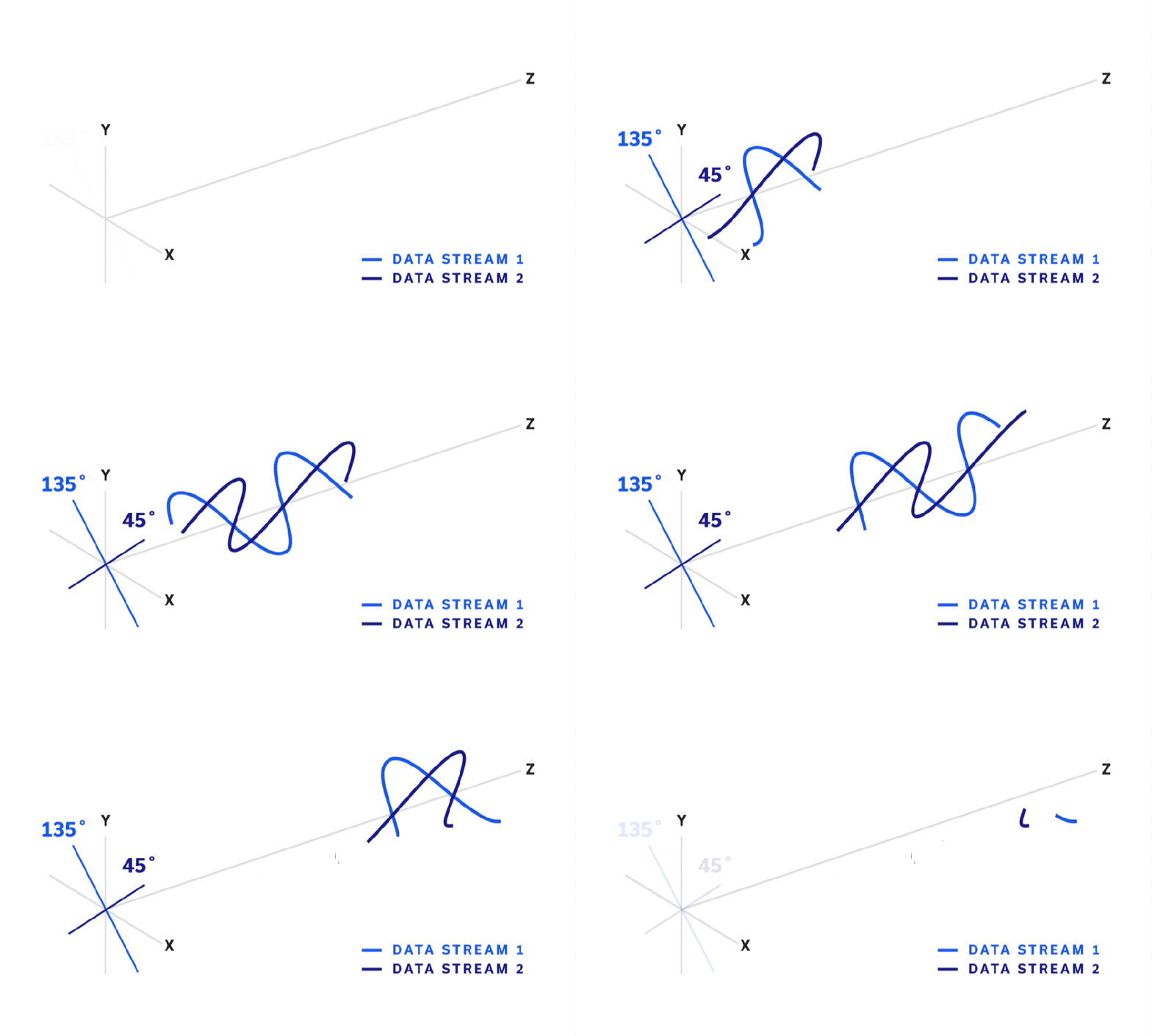
In modern radio communications (particularly commercial cellular and Wi-Fi), Multiple-Input, Multiple-Output (MIMO) is a common method of utilizing multiple transmitting and receiving antennas to increase the capacity of the radio link, reduce errors, and maximize speed. As user demand for bandwidth and data speed have grown, MIMO systems have been integral in the evolution of modern communication systems including cellular communications, Wi-Fi networks and many more.
This article will explore the origins of MIMO technology and explain how concepts of polarization diversity and spatial diversity enable these systems to scale capacity for higher data rates and multiple simultaneous connections to user equipment. Use of MIMO in LTE-Advanced (LTE-A) communications and Wi-Fi 6/6E are then described by way of example.


