RF/Microwave Bias Tees from Theory to Practice
Overview
The bias tee is an essential component for applying DC voltage to any component that must also pass RF/microwave signals, most commonly an RF amplifier that requires a DC supply. For narrowband applications, bias tee design and construction are relatively straightforward, provided attention is paid to component self-resonant frequencies (SRFs). For broadband applications, however, bias tee design and construction are nontrivial, and attention to component characteristics is paramount to a successful, high-performance design. In this article, we examine narrowband bias tee design, component SRFs, and how they impact the design, then extend those ideas to broadband bias tees. We will also compare the electrical and physical performance attributes of different types of broadband bias tee designs including discrete circuits with conical inductors as well as MMICs.
Basic Functions of RF Bias Tees
Bias tees are utilized anytime the designer is required to apply DC bias to an RF line. This is common practice in remote RF electronics where it is generally far more efficient, in terms of both size and cost, to run the DC current up the center conductor of a coaxial cable to power the remote equipment than it is to run separate wires for power supply alone. Bias tees in remote systems of this nature are commonly high-performance, connectorized modules.
Bias tees are also found in “local” applications on high-density, RF/microwave/millimeter wave circuit boards that have dozens of these devices, each occupying only a handful of square millimeters. Figure 1, while not to scale, shows the contrast between two equivalent, ultra-wideband (1.5 to 28 GHz) bias tees, the Mini-Circuits’ MBT-283+ MMIC on the left, and the connectorized ZBT-K283+ on the right.
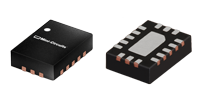
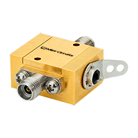
Figure 1: Two of Mini-Circuits’ ultra-wideband (1.5 to 28 GHz) bias tees: the MBT-283+ MMIC (left) and ZBT-K283+ (right).
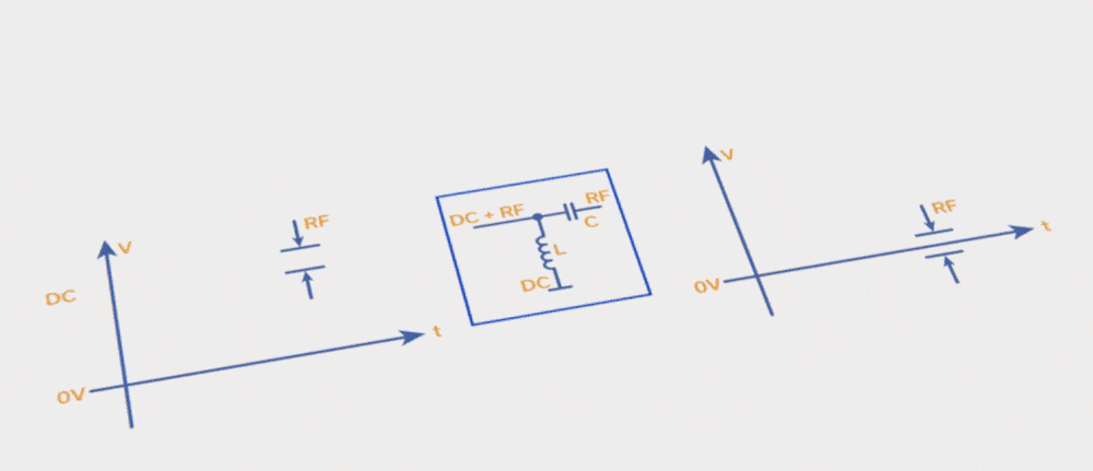
Figure 2 shows a fundamental bias tee configuration. In its most elementary form, the bias tee itself is comprised of just two components, an inductor and a capacitor. DC is fed into the bias tee through inductor L, joining the horizontal RF line which crosses the “tee”. A blocking capacitor C prevents the DC on the lefthand side of the RF line from passing to the righthand side. Figure 2 also shows the respective signals present at the RF input (lefthand side), DC input (bottom), and RF output (righthand side).
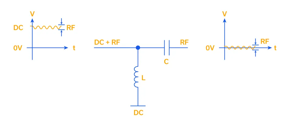
While two components may seem rather skimpy, bias tees have been designed using just an L and a C for decades, particularly in narrowband designs. The concept is quite simple. The lower the frequency, the lower the reactance of the inductor, jωL, such that at DC (ω = 0 rad/s), the inductor is a short-circuit (0Ω). At the frequency of the RF signal, the inductive reactance jωL is designed to be high enough so as to behave like an open circuit (i.e. at least an order of magnitude greater than 50Ω). This way, the inductor passes DC to the RF line while minimizing disturbance to the RF signal, presenting as insertion loss.
The blocking capacitor, as the name implies, blocks DC from being passed to the RF port and subsequent components down the signal chain. To couple the RF signal effectively, a capacitance value is chosen such that the capacitive reactance of 1/jωC is sufficiently low at the frequency ω (i.e. at least an order of magnitude less than 50Ω) so as not to impede the signal and create excess insertion loss.
Component Characteristics and Effects on Bias Tee Performance
For the time being, let’s limit our discussion on bias tee sub-components to narrowband designs. Two rules of thumb ensure good performance in narrowband bias tees (10-30% BW). The first rule is to fully consider the DC component ratings (current for the inductor, voltage for the capacitor) and ensure that the bias tee operating point falls safely below those values. While inductor DC current is fairly straightforward, the voltage across the capacitor is comprised of both an AC and DC component, and the composite peak voltage must be considered. RF/microwave capacitor voltage ratings are quite strong in this day and age, and will generally meet the requirements, but bias tees in RF power amplifier applications will sometimes push the envelope of those standard ratings and require even higher-voltage capacitors to perform the DC blocking function.
The second rule of thumb is to always operate the components below their respective self-resonant frequencies. For the inductor, manufacturers provide this information in the component data sheet. For the purpose of our discussion, inductor self-resonance is always the first self-resonance, and is always parallel resonance. The windings of an inductor present a number of capacitive effects that we refer to collectively as interwinding capacitance. This capacitance is in parallel with the inductance as shown in Figure 3. Likewise, the windings also have some finite amount of resistance, called ESR (Equivalent Series Resistance). This distributed element is also in parallel with the inductance. While ESR does not affect the resonant frequency shown in the equation on the right side of Figure 3, it does affect the Q of the resonance.
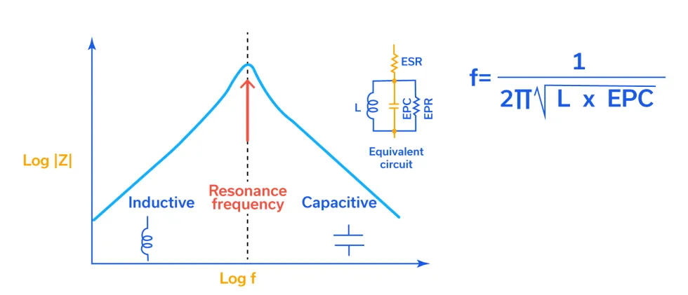
Notice that until the resonant frequency is reached, the inductor behaves much like an ideal inductor insofar as the inductive reactance, jωL increases linearly on a log-log scale. This is the region in which the inductor should be operated for bias tee applications. At the resonant frequency, recall that the theoretical impedance of a parallel L-C circuit is infinite. In Figure 3, however, the resistances ESR and EPR (predominantly ESR) damp this effect, and the impedance is finite. Beyond self-resonance, parallel resonance, or the first resonance, all terms which apply to this condition, the impedance of the inductor becomes capacitive, essentially declining linearly with frequency on the log-log plot of Figure 3.
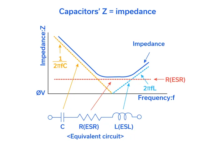
Similarly, a physical capacitor has a self-resonant frequency above which its impedance changes from capacitive reactance to inductive reactance. The capacitor’s self-resonance is a series resonance for which the impedance should reach 0Ω. The dashed line in Figure 4 shows the impedance reaching 0Ω, while the solid line shows the effect that ESR has in damping the resonance. The ESL (Equivalent Series Inductance) is generally very small, typically less than 1 nH for capacitance values less than 1 μF.
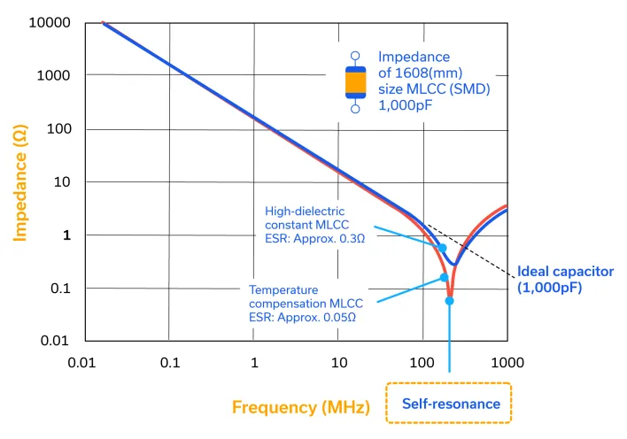
Impedance vs. frequency curves for surface mount, 0603, 1000 pF capacitors are shown in Figure 5. Note that the capacitor with the lowest ESR value (0.05Ω) has the sharpest resonance (i.e. highest Q). Additionally, notice how the capacitors both deviate from ideal beyond resonance, their respective impedances both beginning to follow an inductive reactance curve. This is why it is critical to operate the capacitor below its self-resonant frequency when designing a bias tee.
There you have it: two rules-of-thumb, two components, and one narrowband three-port bias tee. It’s essentially a review of real RF component characteristics – that is until we turn our attention to broadband bias tees.
Broadband Bias Tees
Wideband Capacitors
Decades ago, perhaps one of the first practical lessons a circuit designer would learn at the outset of their career was the art of decoupling using a combination of different value capacitors. A good mentor would explain that because of their physical characteristics, different value capacitors were optimal for filtering different frequency bands. This author even remembers designing a decoupling network for a 25W buck converter that included the parallel combination of ceramic capacitors of 1 μF, 0.1 μF, 0.01 μF, and 1000 pF in value. The network performed well once the component leads were made short enough!
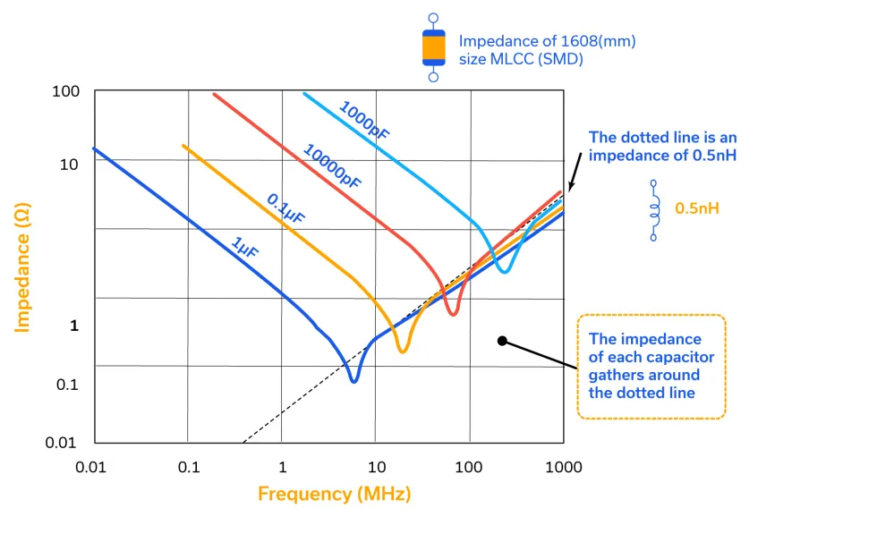
Although the capacitors of yesteryear had radial leads, the reason that particular combination of capacitor values performed well in decoupling to ground (and would also perform well in AC coupling, as with a DC blocking capacitor) is that each value has its own, unique self-resonant frequency, as shown for the 0603 surface mount capacitors in Figure 6. Combining all these disparate self-resonant frequencies together in parallel yields a relatively broad band of frequencies over which the parallel capacitance network exhibits very low impedance. Nevertheless, the physical effects of capacitor construction include ESL, and the impedance beyond resonance for each capacitor value invariably follows an inductive reactance curve.
Wideband RF/microwave capacitors take advantage of the different response characteristics for capacitors of different values. A number of different values are “baked into” a single SMT chip capacitor, enabling the capacitor to perform very well over many octaves. It appears that the first patent for a component construction of this nature was issued in 2005 to Daniel, Alan, and Lambert Devoe.4 One must assume that the patent was licensed, since wideband 100 nF microwave capacitors have been available for well over a decade. While the patent may have expired in 2022, the utilization of wideband microwave capacitors continues to increase, and the characteristics of these components continues to improve over time. In fact, the Kyocera AVX 550L and 560L series of 0402 ultra-broadband capacitors exhibit flat frequency response from 16 kHz through 70 GHz and 40 GHz, respectively.
Broadband (Conical) Inductors
In the realm of RF/microwave inductors, the broadband conical inductor is the counterpart to the wideband capacitor. While wideband (or ultra-broadband) capacitors have come into vogue in the last decade and a half, it is not exactly clear when the conical inductor was invented or when they became popular. Perhaps the reason is that right after the pioneers that helped us understand inductors, Hans Oersted, Andre Ampere, and Michael Faraday, came Nikola Tesla whose famous Tesla transformer was finalized by Tesla in a conical shape. While Tesla’s aim was not to reduce parasitic capacitance of the Tesla transformer, he certainly had utilized the conical shape before anyone else (1891). In fairness, there was a patent issued in 2009 to Uriel Fojas (assigned to Agilent Technologies Inc.) covering a small conical inductor structure.5 Today, multiple suppliers provide tiny, broadband conical inductors for use in discrete bias tee and filtering implementations.
The conical shape greatly reduces interwinding capacitance and the large turns carry the lower frequencies while the small turns the higher frequencies, making for an excellent broadband inductor. John Dunn does an excellent job of describing both physically and mathematically the advantages of a conical inductor in his article on January 30, 2023 in EDN.6
Discrete Broadband Bias Tees vs. Integrated Bias Tees
Wideband RF/microwave capacitors and broadband conical inductors can certainly be combined to form a worthy, discrete, broadband bias tee. Prior to wideband capacitors and conical inductors, one option was to design the bias tees in stages, utilizing multiple inductors and capacitors to broaden the BW. Physically, that is a cumbersome approach, and from a cost perspective, impractical.
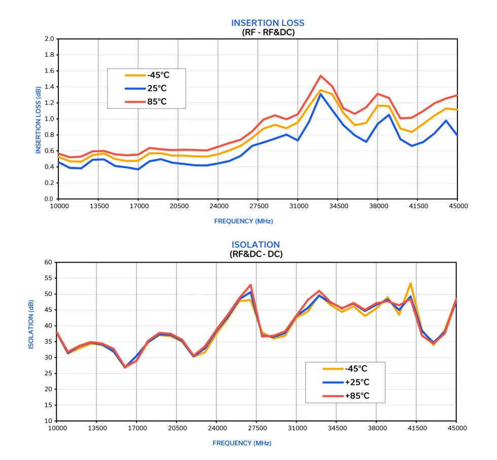
Even a lone conical inductor is complicated to mount on the circuit board. The terminals are the same fine wire that is used to wind the inductor, and must be attached to very narrow pads to keep parasitic capacitance to a minimum. This alone poses significant challenges for reliability and repeatability at higher volume. Secondly, the mounting angle for the inductor must generally be between 45 and 60 degrees to horizontal, again, to keep parasitic capacitance from defeating the purpose of using a conical inductor in the first place. To be fair, plastic housings can now maintain the angle of the conical inductor as they are reflowed to the circuit board, which helps mitigate improper installation. In many cases, however, conical inductors with plastic housings cannot be reworked, as the plastic may soften or burn with the application of a localized heat source. Nevertheless, discrete L-C bias tees can operate from frequencies in the 10’s of MHz to the order of 40 GHz, often well in excess of the bandwidth of other components in the system, such as LNAs for receivers or predrivers in integrated/distributed power amplifiers. In these cases, an integrated, MMIC bias tee is a more desirable and effective approach. Consider Mini-Circuits’ MBT-283+ MMIC bias tee shown in Figure 1. This model operates from 1.5 to 28 GHz, supports 500 mA of DC bias current and has physical dimensions of just 3.5 x 2.5mm. The MBT-44+ MMIC bias tee (Figure 7) operates from 10 to 40 GHz, also supports 500 mA, and measures just 2.5 x 2.5mm. In addition to its compact size, the MMIC device exhibits low insertion loss and high isolation across the band. If contiguous bandwidth from tens of MHz through mmWave is not required for a given implementation, MMIC bias tees are a superior option given their cost-effectiveness, inherent reliability and manufacturability.
Summary
Bias tees in their most basic form are very simple devices consisting of nothing more than an inductor and a blocking capacitor. As we review the self-resonant characteristics of both physical inductors and capacitors, it becomes clear that broadband bias tees are more complex, often requiring several stages of L’s and C’s to achieve the desired performance. Alternatively, the use of conical inductors combined with wideband capacitors can also achieve the same design goals. Discrete bias tee designs may be necessary in cases where the designer needs to carry the VHF/UHF portion of the band. These approaches, however, sometimes carry practical limitations with respect to board real estate, manufacturability and cost as bandwidth extends to higher frequencies.
MMIC bias tees such as the MBT-283+ and MBT-44+ discussed in this article offer broadband performance into the millimeter-wave range in a small, surface-mountable form factor with exceptional reliability and repeatability. These devices are compact, and exhibit high isolation and low insertion loss. Connectorized bias tees are also available from Mini-Circuits for coaxial assemblies or biasing amplifiers in the lab environment.
View Mini-Circuits’ full selection of RF Bias Tees >
References
- Frequency-Impedance Characteristics of Inductors and Determination of Inductor’s Resonance Frequency | Dealing with Noise Using Inductors | TechWeb (rohm.com)
- Fundamentals of Capacitors and Hybrid Capacitors – Panasonic
- EMI suppression filters 6 | Noise Suppression Basic Course | Murata Manufacturing Co., Ltd.
- US6970341B1 – Integrated broadband ceramic capacitor array – Google Patents
- US20060139124A1 – Circuit assembly with conical inductor – Google Patents
- A look at conical inductors – EDN


