Measurement of Amplifier Additive Phase Modulation Noise (APM)
Part 1: Background & Theory
Optimum APM Test Configuration
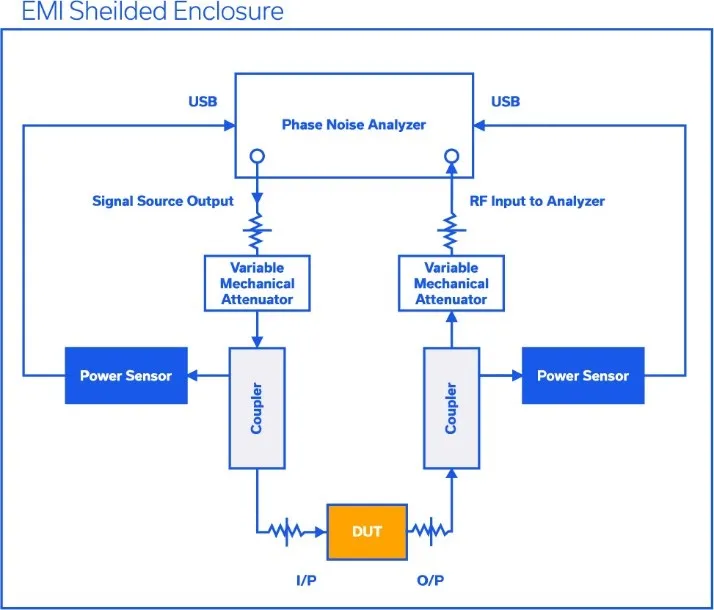
In our efforts to properly characterize the Additive Phase Modulation Noise (APM) and Additive Amplitude Modulation Noise (AAM) performance of MMIC amplifiers in our labs, Mini-Circuits is careful to consider the performance capabilities and limitations of our phase noise analyzer and test setup (see Figure 4). Both APM and AAM performance can be dependent upon the analyzer’s internal signal source carrier frequency, power level, and, importantly, the phase length from signal source output to RF input, so great care must be taken to optimize these parameters.
For example, at a carrier frequency of 2 GHz, the measured APM and AAM performance of our analyzer’s internal signal source is well-behaved for all power levels, +13 dBm (the maximum available) and below. However, at other carrier frequencies, 4 GHz for example, AM-to-PM distortion associated with the internal signal source requires that the maximum level be reduced to below approximately +10 dBm to obtain optimum APM performance. This dependency could limit the input power dynamic range to the device under test (DUT), and therefore the output power available from the DUT.
Additionally, we have identified that for our analyzer, fixing the signal source power at the optimum level and using an external, mechanical step attenuator and fixed pad on the signal source output port to set the power level into the DUT, provides improved APM performance compared to that achieved using the analyzer’s internal attenuator. We use a second mechanical step attenuator and fixed pad after the DUT, on the input to the analyzer’s RF input port and adjust the attenuation to maintain a constant signal power into the analyzer’s RF input port. This method provides for enhanced accuracy and repeatability and ensures that maximum input power levels are never exceeded. Ideally, the RF input port signal power is adjusted and maintained at a fixed power level, between ≈+7 to +13 dBm for all input attenuator steps.
Importantly, it has long been established that for any carrier frequency and power level considered, the longer the phase length between the analyzer’s signal source output and RF input ports, the more degradation that could result in APM for offset frequencies above approximately 300 kHz. This is because the phase noise analyzer cannot properly cross-correlate the two pairs of baseband inputs when the phase variation of the carrier is too rapid (decorrelation). As a result, the analyzer interprets the two pairs of baseband inputs as uncorrelated and will add this noise back into the measurement. To mitigate this effect, it is important to minimize the phase length between the analyzer’s signal source output and RF input ports. This effect is not unique to the phase noise analyzer used in Mini-Circuits’ test setup, and similar measures should be taken in test sets using other analyzers as well.
DUT Characterization
Amplifiers are typically characterized over an input power dynamic range of ≈20 dB. This range is usually sufficient to operate the amplifier from small signal to 3 dB gain compression. However, achieving this may not be possible for all DUTs, as the RF input power test parameter is a function of the DUT performance, the test setup losses, and the maximum signal source power available from the phase noise analyzer.
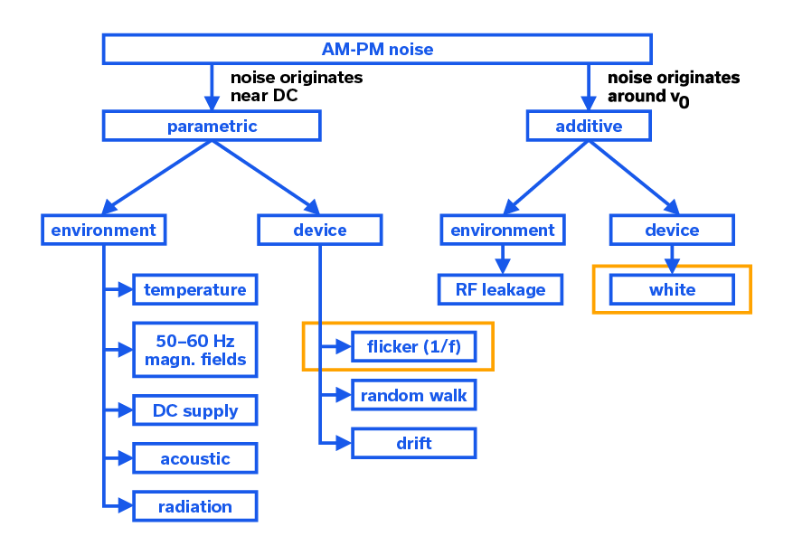
Characterization over this dynamic range also ensures that both white (additive) and flicker (parametric) phase noise effects are adequately addressed because, in amplifiers, these are the dominant contributors to short-term phase noise.
Case 1: Small Signal Region (~10 dB fixed pad on Signal Source Output Port).
For this case, we begin with the lowest DUT input power to be used and incrementally increase the power level by reducing the input mechanical step attenuator value in 1 dB steps, over a 10 dB dynamic range. The DUT output power is adjusted using the output mechanical step attenuator and fixed pad to maintain the signal at a fixed power level between +7 dBm and +13 dBm (ideally), for all input attenuator steps.
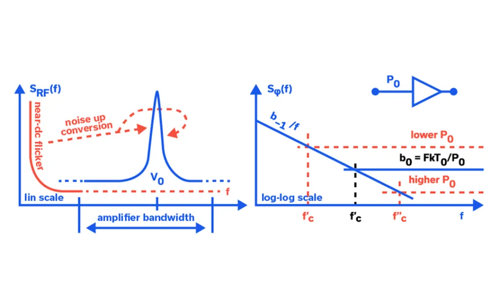
If the setup is configured and operating correctly (see Figure 2) one should observe an improvement in APM for offset frequencies above ~100 kHz as the DUT input power is increased from the minimum. This is because under small signal operation and in the additive (noise originates around the carrier), white noise region, Sф(f) [rad2/Hz], the power spectral density of the random phase, ф(t), decreases with increasing input power level. In this region, the additive phase noise spectrum is defined by the following relationship:
Sф(f) [rad2/Hz] = b0 = FkTo/Pin and L(f) = ½ Sф(f)
L(f), the additive phase noise, is related to Sф(f) by a factor of ½. It is typically expressed as L(f) [dBc/Hz] = 10*LOG10(L(f)). Pin [W], is the power of the input signal, F[-] is the noise factor of the amplifier, To is the reference temperature of 290K, k is Boltzmann’s constant and f [Hz] is the offset frequency from carrier. [1].
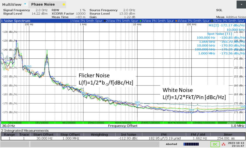
White (>≈100 kHz offset), additive (originating around the carrier) phase noise, may also be expressed in terms of the amplifier’s input power, Pin[dBm], and noise figure, NF[dB], and is related to the power spectral density of phase fluctuations (-177dBm/Hz) by the following formula:
L(f) [dBc/Hz] = -177 [dBm/Hz] +NF [dB] – Pin [dBm]
The above is frequently used to derive the amplifier’s noise figure under drive, but may be limited by the test equipment noise floor and other effects (phase length, sampling rate), unrelated to the amplifier’s actual NF performance. It is not unusual for the DUT’s noise figure under drive to vary significantly from the small signal noise figure, measured with a noise figure meter, as result of increasing non-linear distortion with increasing input power.
Case 2: Large Signal Region (~0 dB fixed pad on Signal Source Output Port).
We begin with the last DUT input power used in Case 1, and incrementally increase the power by reducing the input mechanical step attenuator value in 1 dB steps, over a 10 dB dynamic range. The DUT output is adjusted using the output mechanical step attenuator and fixed pad to maintain the signal at a fixed power level between +7 dBm to +13 dBm (ideally), for all input attenuator steps.
As DUT input powers increase, the amplifier’s gain will begin to compress. Ideally, the input dynamic range should be sufficient to drive the amplifier to at least 3 dB of gain compression. Depending upon certain immutable characteristics of the amplifier under test, APM may ultimately achieve a minimum level at some specific (“optimum”) input power level and offset frequency. This optimum input power level typically corresponds to the amplifier’s input 1 dB compression point, ±3 dB. However, there is no general rule that can be applied to all amplifiers specifying what this optimum input power will be, or if it even exists. It is dependent upon device technology, semiconductor material, DC bias circuit design, amplifier topology, linearity (IP2, IP3) and large signal behavior (AM-to-PM and other non-linear distortions) and must be determined through testing.
Unlike white noise, near baseband, parametric (originates near-DC), flicker or 1/f noise, is mostly independent of carrier power (see Figure 2) and is directly upconverted to the carrier frequency, largely independent of the actual carrier frequency. It is caused by a near-DC noise modulating the phase, frequency or amplitude of the passing carrier and the I/O impedances of the amplifier. 1/f noise (<≈100 kHz offset), commonly associated with certain device technologies (pHEMT, HBT, BJT), gate lengths (0.5, 0.25, 0.15, 0.1 um) and semiconductor materials (GaAs, Si, SiGe, InP, GaN) is generated in the amplifier and the DC bias circuitry. In this region, the additive phase noise spectrum is defined by the following relationship:
Sф (f) [rad2/Hz] = b-1 / f and L(f) = ½ Sф(f)
Combining the white and flicker regions into a single relationship yields the following:
Sф(f) [rad2/Hz] = b0 + b-1 / f and L(f) = ½ Sф(f)
With b0 = FkTo/Pin and b-1, determined through measurement.
These two effects may be visualized using Figure 2, courtesy of Boudot, Rubiola, and Rohde, Rubiola, Whitaker, respectively [1]:
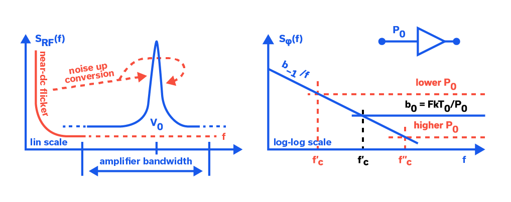
Note that because near dc, 1/f noise is transferred to a carrier via an up-conversion process, it is typically not required to test the amplifier at multiple carrier frequencies, provided the amplifier’s performance is relatively consistent over its band of operation. Unfortunately, for very wideband amplifiers this may not always be the case and measuring performance over a wide range of increasing carrier frequencies may be required. While doing this, we have found that measured APM performance may be influenced or even limited by the test equipment’s noise floor and that results may not always reflect the true performance of the amplifier.
[1]. The original definition of L(f) (circa 1970) assumed the power in the noise sidebands was much smaller than that of the carrier, was based on the use of a spectrum analyzer, and was defined as the power in a 1 Hz bandwidth at a frequency, f, offset from the carrier frequency, f0, divided by the carrier power. In 1988, the IEEE Standard 1139 replaced this obsolete definition with ½ S(f), but the former is still widely utilized. There are many reasons why the obsolete definition is both conceptually and experimentally incorrect, one of the more obvious being that AM and PM noise cannot be identified individually. The interested reader is referred to “Microwave and Wireless Synthesizers, Theory and Design, 2nd Edition”, by Rohde, Rubiola and Whitaker.
Determination of Maximum Source Level for Acceptable APM Performance and System Noise Floor
Before initiating a DUT measurement, it is prudent to characterize the analyzer’s internal signal source for APM/AAM performance and to establish the system noise floors. To accomplish this, the DUT RF input port is connected to the DUT RF output port using a through adapter. The analyzer’s signal source power level is first set to the maximum, +13 dBm for our analyzer, and the signal frequency is set to the carrier frequency of interest. Each mechanical step attenuator is set to the minimum attenuation step and the fixed pads are adjusted so the analyzer’s signal level is approximately the same as that expected from the DUT. Once this has been accomplished, the APM measurement may be initiated.
Once a sufficient number of cross-correlations have occurred, the results are examined and a determination is made as to whether the performance is acceptable for the specific amplifier under test. AM-to-PM distortion, for example, typically manifests as excessive APM and peaking for offsets below approximately 400 Hz, but higher offset frequencies could also be affected.
If performance is determined to be acceptable, this process is repeated for all carrier frequencies of interest before proceeding to the DUT characterization phase.
If performance is not acceptable, the analyzer’s internal attenuator should be used to reduce the signal source power level in 1 dB steps until the desired performance is achieved. This level represents the maximum that can be used in characterizing the DUT at that specific carrier frequency.
DUT Characterization Procedure for APM and AAM Performance
DUT characterization may proceed at this point and is covered by the subsequent article in this series.
