RF Pulse Modulation: Fundamentals, Applications & Design Techniques
Early Pioneers of RF Pulse Modulation
Pulse modulation has been around for over 125 years. In 1887, German physicist Heinrich Hertz built the first experimental spark-gap transmitters (electromagnetic pulse modulators), with which he proved the existence of radio waves.1 In 1888, using 455 MHz radio waves, he studied the ability of radio waves to be reflected from metallic objects and refracted by dielectric media.2 Hertz confirmed James Clerk Maxwell’s work from 1865, which was simplified by Oliver Heaviside in 1884. Hertz’s work also spawned early target detection when, in 1904, a patent for “an obstacle detector and ship navigation device,” based on the principles demonstrated by Hertz, was issued in several countries to German Engineer Christian Hülsmeyer.2 Hülsmeyer’s British patent (September 23, 1904) was for a spark-gap-type, full 600 MHz pulsed radar system that he called a telemobiloscope.3
Subsequent radar system development took place in many countries, but about three decades after Hülsmeyer’s patent, Robert Watson-Watt of Great Britain’s Air Ministry played a key role in ensuring the deployment of radar systems along the East and South coasts of England in time for the outbreak of World War II in 1939, a collection of stations known as “Chain Home”.3 Once Winston Churchill approved Henry Tizard’s mission to transfer technology secrets to the United States in 1940, a trunk containing those secrets was entrusted to Edward George Bowen, who almost lost sight of it in transit at Euston Station.4 When the British scientists’ American counterparts saw the performance of the compact 3 GHz, 10kW cavity magnetron known as “Number 12” developed by John Randall and Harry Boot, they were stunned, as their own efforts had stalled.4 In the years that followed, one million of these magnetrons would be produced in the United States,4 many installed in Allied fighter and bomber aircraft, ushering in the age of the airborne early warning radar system.
These stunning early achievements and those whose work went into them opened the door to the sophisticated radar systems of today. But radars are only one application of pulsed RF modulation. This versatile modulation scheme is used in applications as various as high-energy physics experiments, electronic warfare and avionics. Medical applications include the treatment of tumors, cardiac arrhythmias, pain, edema, bone fractures, and soft tissue wounds. Even magnetic resonance imaging (MRI) depends upon pulsed RF modulation. In what follows, we will study the fundamentals of the pulsed signal itself, as well as the application of a pulsed envelope to an RF carrier waveform. Finally, we’ll address practical ways of creating pulsed RF waveforms utilizing some of the more common families of parts from Mini-Circuits.
Pulse Waveform Basics
The single, rectangular pulse extending from -τ/2 to +τ/2 and having an amplitude A appears in the time domain and has the Fourier transform (frequency domain equivalent) shown in Figure 1.5 The magnitude of the Fourier transform, often referred to as the amplitude spectrum, is also shown in Figure 1.5 The Fourier transform of the rectangular pulse takes for the form of sin(x)/x, or the sinc(x) function. The detailed computation of the Fourier transform and its coefficients can be found in reference [6] below.
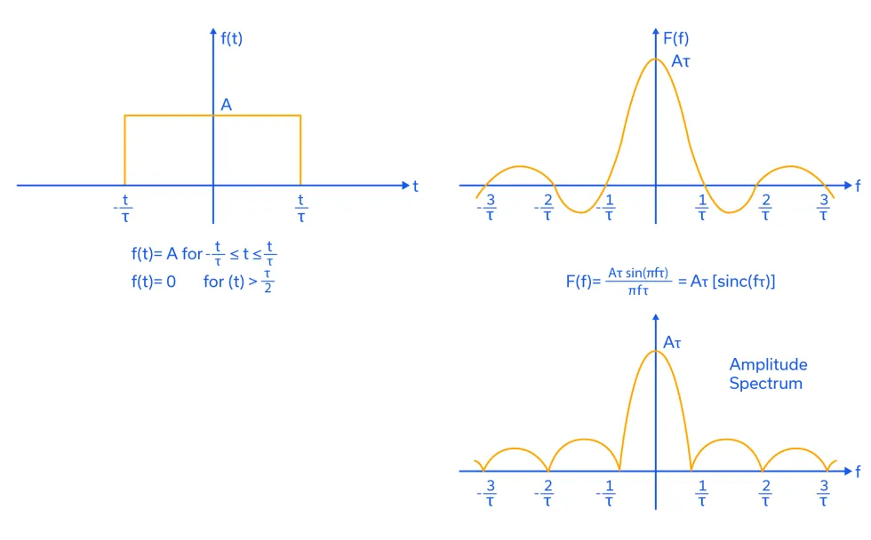
In the frequency domain, the amplitude of the spectrum is a maximum of Aτ at f=0, and declines with increasing or decreasing f ad infinitum. Yes, a rectangular pulse in the time domain has infinite bandwidth in the frequency domain. While it is clearly undesirable for any real RF system to occupy infinite bandwidth, keep in mind that this is also true only if the rise and fall times are zero, which is theoretically impossible.
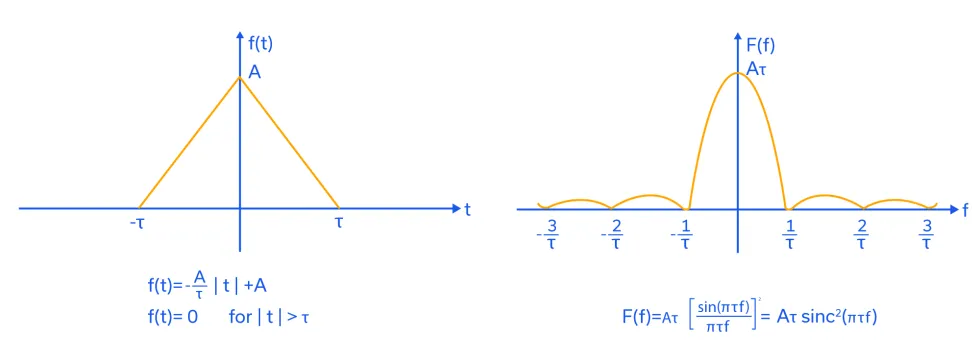
What happens to the amplitude spectrum in the frequency domain if the rise and fall times are finite? Take the extreme case of the triangular pulse in Figure 2. The rise and fall times of the waveform are A/τ and -A/τ on the negative and positive sides of the y-axis, respectively. Note first that the Fourier transform is now the sinc2(x) function (always positive), and consequently equivalent to the amplitude spectrum. Secondly, the amplitude of the maximum at f=0 (the “main lobe”) is still Aτ, but the amplitude of the maxima on either side of the main lobe (the “side lobes”) declines far more dramatically when compared to the spectrum of its rectangular pulse counterpart in Figure 1. This frequency domain phenomenon, albeit achieved by radically slowing the rise and fall time, is known as “sidelobe suppression.” The advantage of sidelobe suppression is the utilization of less frequency spectrum for system operation; the disadvantage is that less precision is available in the detection of the leading and falling edges of the pulse.
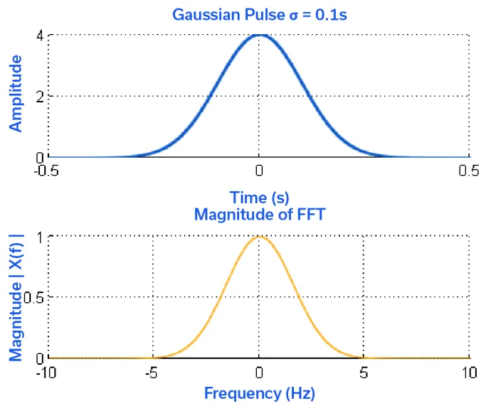
Taken to yet another extreme, the Gaussian pulse can be shown to have a Fourier transform that is itself a Gaussian pulse, or Gaussian-shaped spectrum, as shown in Figure 3.7 The computation of the Fourier transform is also included in reference [7]. This type of pulse shaping may be used to further limit the occupied bandwidth of a system.
RF Pulse Modulation
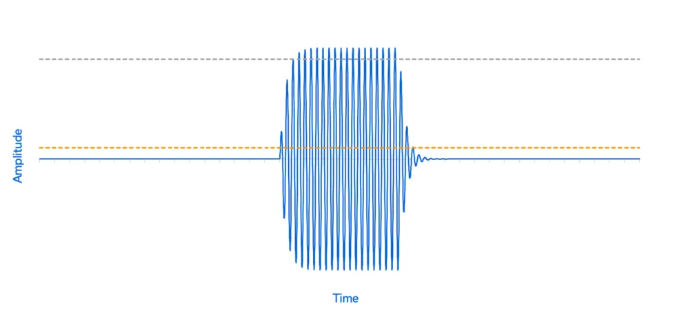
Figure 4 shows a simplified time domain representation of a pulse-modulated RF signal. The pulse width is determined at the 50% point of the voltage scale, or where the waveform crosses 0V. The rise and fall times are each approximately 2 ns. Often, when examining pulsed RF waveforms in the time domain, it is useful to employ a voltage detector so that only the envelope is shown. Figure 4 was rendered so that the reader can see the entire construct of the pulsed RF signal.
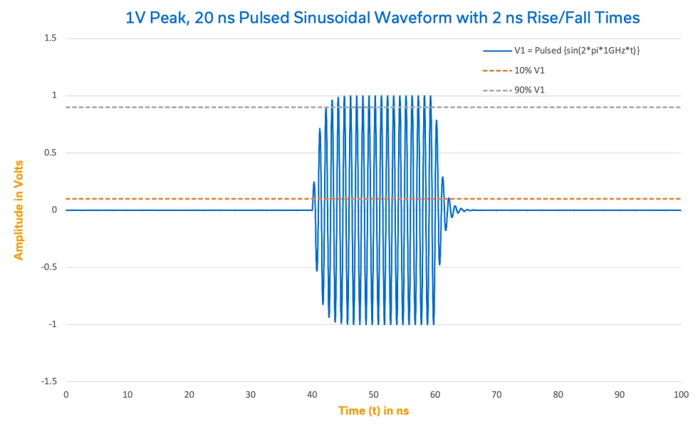
Figure 5 exhibits the amplitude spectrum of a similar signal in the frequency domain with 1W (30 dBm) pulses, a pulse repetition frequency (PRF) of 1 MHz, and zero rise and fall times. Note that the power level of the peak of the main lobe appears below 0 dBm which differs considerably from the nominal power of the pulse. Since the pulsed signal has its power distributed over a large number of spectral components or “lines” (i.e. each marker on the plot is effectively the tip of a vertical line in the Fourier transform), and each component represents a small fraction of the peak pulse power, we must use what is known as the pulse desensitization factor, αL,8 defined as:
αL = 20log (duty cycle)
For the 30 dBm, 20ns pulse at 1 MHz PRF, we have:
αL = 20log(20 ns/1 μs) = 20log(0.02) = -33.98 ≈ -34 dB
Applying the desensitization factor -34 dB to the 30 dBm pulsed waveform results in -4 dBm, which corresponds to the maximum of the main lobe in the spectrum profile in Figure 5.
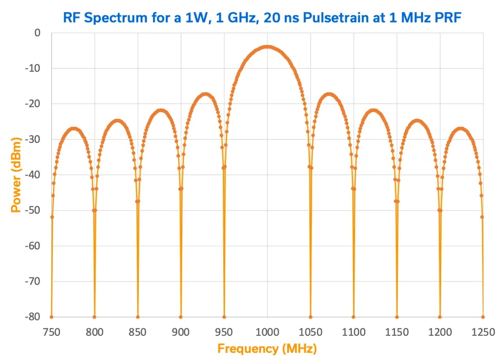
Notice that the spacing between the markers, or spectral lines in the plot is exactly 1 MHz, equal to the PRF (sometimes referred to as the “rep rate”). Additionally, the width of the sidelobes is the reciprocal of the pulse width, such that:
Pulse width = 1/lobe width = 1/50 MHz = 20 ns
Legacy RF Pulse Modulation Applications
Decades ago, military test ranges were bustling with activity. Highly maneuverable unmanned target drones designed to be engaged by fighter jets were flown by operators on the ground often, using modulation schemes no more sophisticated than pulse position modulation or pulse code modulation. These on-off-keying (OOK) systems were effective for command and control at long range due to the output power of both the ground-based and onboard transponders. Some drone telemetry even worked its way back to the ground using RF pulse modulation. One function on the U.S. test ranges of the 1980s and 1990s relegated to RF pulse modulation was the range safety function known as radar tracking.
High-power transmitters on the ground transmitted pulses to a drone’s onboard radar tracking transponder and received a high-power, pulsed response. Two workhorses of that era were the U.S. Navy AN/DPN-90(V)1 (5.4 to 5.9 GHz) and the AN/DPN-90(V)2 (9.0 to 9.5 GHz) radar tracking transponders. Their magnetron-based transmitters coupled many hundreds of Volts from a pulse transformer to the cathode of the magnetron to transmit 0.5 μs pulses measuring hundreds of Watts, making it easier to keep track of multiple flying drones and aircraft simultaneously.
Military test range safety has changed dramatically in recent decades due to the maturation of GPS-based tracking, more sophisticated and capable radars, and the sheer variety and preponderance of UAVs. Commercial avionics, however, still requires a transponder, most often operated in mode S by passenger aircraft companies. These systems generally transmit 200W pulses, each transponder at a unique “squawk code” and at a transmit frequency of 1090 MHz. Mode S was developed in 1975 at MIT Lincoln Labs and is being used not just to make the aircraft easily identifiable, but in collision avoidance as well.
RF Pulse Modulation: Practical Implementations
The Traditional RF Switch
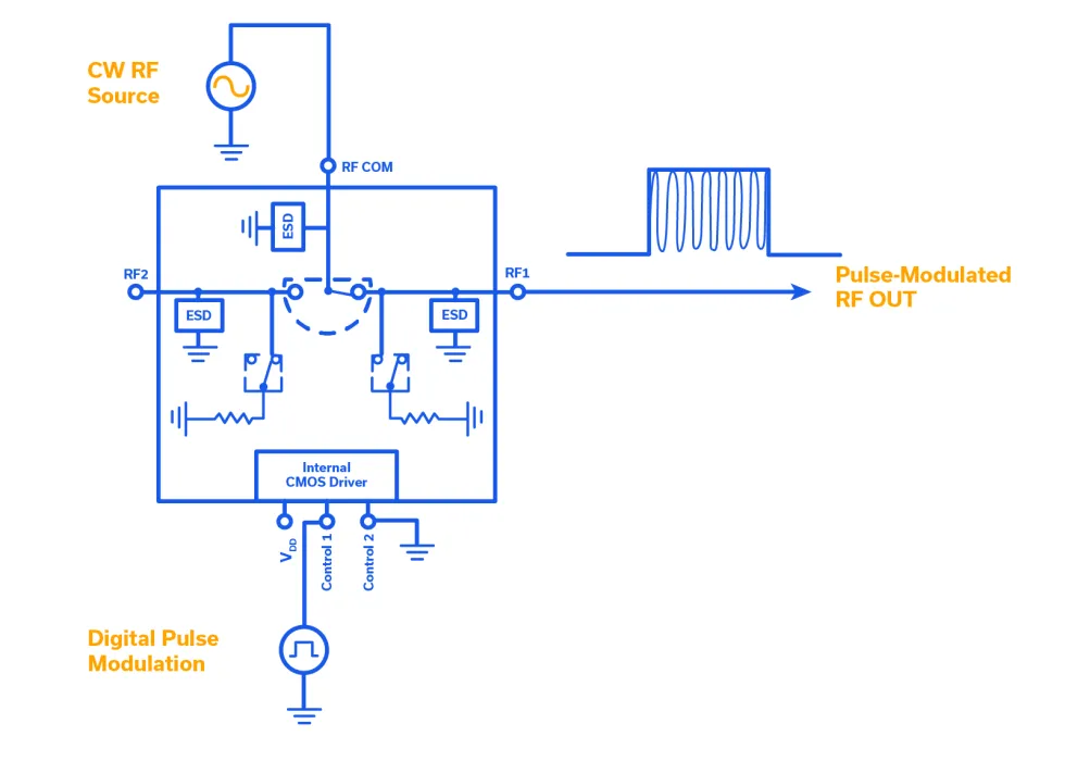
In a physical sense, there are a variety of ways to create pulsed RF signals. Perhaps the simplest way is to start with a CW source, insert a simple single-pole, double-throw (SPDT) RF switch in-line, and toggle the switch with digital pulses. Amplification can follow to achieve the desired RF power level. Figure 6 illustrates this method of RF pulse generation utilizing a Mini-Circuits’ HSWA2-63DR+ surface-mount MMIC SPDT absorptive switch, which operates from 100 MHz to 6 GHz. CW is present at the common port, and the switch state toggles between RF 1 and OFF according to the state of Control 1 and Control 2 as shown in the truth table on the model datasheet. The insertion loss of the switch is typically 1 dB between 2 and 3 GHz, while isolation is typically 62 dB. High on/off isolation is commonly found in absorptive switches since, in the off position, the switch ports RF1 and RF2 are terminated internally, as shown in the schematic. While the delay from the control inputs to RF switching is typically 300 ns, the rise and fall times are impressive at 67 ns. If high on/off isolation is not required, reflective switches such as the MSW2-50+ can provide switching at almost instantaneous speeds of 4 ns rise time and 7 ns fall time. Insertion loss for the reflective switch is still 1 dB between 2 and 3 GHz, and isolation is still quite good at approximately 40 dB.
Solid State RF Amplifier Bias Control
Just as high-energy pulses into the cathode of a magnetron can create high-power RF pulses, so can the on/off switching of bias conditions in solid-state amplifiers. Since the advent of commercially available, high-power LDMOS and GaN just after the turn of the 21st century, many systems over the last 2 decades have adopted a solid-state approach and undergone RF tube replacement. Solid-state devices are far and away more reliable than their tube counterparts and with LDMOS and GaN power devices, usually more efficient.
Creating a high-power, pulsed RF source requires, first and foremost, a stable CW source. An abundance of stable TCXO, VCXO, VCSO, DRO, etc. components are available on the market, and we’ll simply assume any one of them to be our CW source for the sake of illustration.
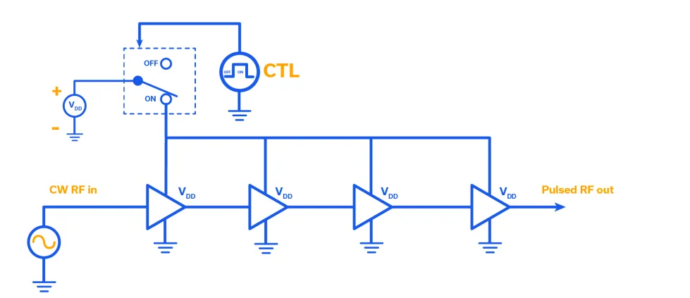
Figure 7 shows a generalized block diagram of a multi-stage amplifier, each stage with an input, output, VDD (bias) pin, and ground. Note that all the VDD pins have been notionally connected and plumbed through an SPDT analog switch. This illustrates the basic concept of bias control. When the analog switch is on, the amplifier is biased, and the CW source is amplified and appears at the output of the final stage. Conversely, when the analog switch is off, all stages of the amplifier are off, and no signal is present at the output of the final stage. Since VDD implies that the drain of a field effect device is being biased, regardless of whether it’s the drain of a GaAs LNA MMIC or that of a high-power GaN MESFET, the method illustrated in Figure 7 is referred to as “drain switching.” While there are faster ways to turn amplifiers on and off, or to pulse modulate CW RF within the amplifier itself, drain switching is a well-known technique that affords well-behaved RF rise and fall characteristics, and rule-of-thumb predictability for on/off isolation at approximately 20 dB per stage.
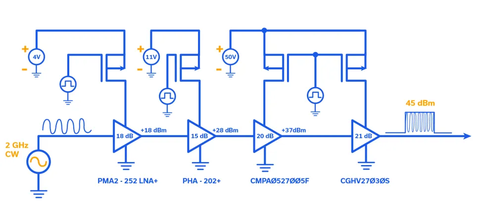
Figure 8 provides a more detailed description of the concept shown in Figure 7. In Figure 8, each device is shown along with its gain, output P1dB, and required drain voltage. The drain voltage is applied to each device through a notional P-channel MOSFET. While P-channel MOSFETs are easier to utilize under certain circumstances such as for low drain voltage devices, once the required drain voltage reaches the order of 50V, an additional component known as a MOSFET driver IC is often designed in. The two main disadvantages of drain switching are that high DC currents often have to be switched by the MOSFETs and the capacitance on the device side of the MOSFET must be limited to only the amount necessary for stable operation.
Another method for creating RF pulse modulation through amplifier bias control is known as “gate switching.” In gate switching, the gate of each field effect device is toggled between a state in which the device is “pinched off” and a state in which the device is biased on at IDQ (quiescent drain current). One primary advantage of gate switching is that the switching networks operate at very low power, moving essentially no current to change the gate voltage. Additionally, large amounts of storage capacitance can be located right on the drain of the RF devices. Finally, rise and fall times can be considerably faster than with drain switching for the same amplifier. One main disadvantage is that the switching of the gate is a delicate operation. For example, the difference between on and off for a device is often just a difference of 0.5V on its gate, and not every device will react the same given the same gate voltage.
Finally, the combination of Figure 6 and Figure 8 often makes for very nice pulsed RF system that switches at blistering fast speeds and has excellent on/off isolation. The RF switch either resides at the input of the RF amplifier or is embedded between lower-power stages. In a system with a priori knowledge that a pulse needs to be generated, gate or drain switching can be used in conjunction with the toggling of an in-line RF switch to achieve both high isolation and optimum rise and fall times.
Modern Day Pulse Modulation Applications
Since its declassification by Lawrence Livermore National Laboratory in the mid-1990’s, the Impulse Radio Ultra-Wideband (IR UWB) system has gained traction in many technologies. Much of the early work in the UWB field prior to 1994, particularly in the area of Impulse Radio, was performed under classified U.S. Government programs. This technology utilizes sub ns pulses, similar in form to the pulse waveforms shown in Figures 1 through 3, rather than a pulse-modulated RF carrier such as that shown in Figure 4. Due to the proliferation of UWB applications, the FCC has allocated the 3.1 to 10.6 GHz in 500 MHz channels to UWB with tight radiation limits, of course, in light of the fact that the emissions are spread over such a broad and densely utilized bandwidth. UWB systems are low power and low cost, and because of the excellent timing constraints that can be placed upon narrow pulses and their returns (echos), UWB systems are highly precise.
It is not uncommon for a UWB system to utilize a pulse of approximately 100 ps and a PRF of anywhere from 1 to 50 MHz. At times, data encoding is even performed using changes in the PRF itself. Specially designed pulse shaping networks ensure that the frequency domain spectral content of these narrow pulses remains within the prescribed bandwidth. While their range is somewhat limited to the tens of meters, due to the transmitted power constraints, these systems have matured through the incorporation of advanced signal processing, and are capable of performing a multitude of functions.

UWB medical imaging has become a focus of much research, with an emphasis on the breast, brain, and heart. UWB (microwave) techniques do not use ionizing radiation like x-rays, so scans can be performed frequently without the exposure risk of traditional imaging methods. UWB technology has also emerged as one of the preferred choices for “see-through-the-wall” precision radar imaging for search, rescue and emergency operations, allowing responders to see the layout of buildings, the presence of persons and potential hazards from the outside.
Radars in the UWB domain have a myriad of military applications like buried land mine detection, ground penetration radars, and material characterization. Experiments have even demonstrated the ability of UWB systems to detect the motion of vocal cords and to perform both speaker verification and speech synthesis nearly instantaneously.
Commercial applications of UWB systems also abound, with real-time asset location within a facility (including employees), ultra high-speed communications, and industrial position sensing to name just a few. The invention of the UWB system is credited to Thomas E. McEwan at Lawrence Livermore National Laboratory in the early-to-mid 1990s.9
No, We’re Not Mentioning Pulsars
In this application note, we first of explored some of the early mathematical, scientific, and engineering pioneers and their respective achievements which brought RF pulse modulation to light. We studied basic waveshapes (rectangular, triangle and Gaussian) in both the time and frequency domains. With an understanding of the mathematics behind us, we illustrated and discussed the characteristics of an RF pulse in the time domain and its corresponding amplitude spectrum in the frequency domain (as it would appear on a spectrum analyzer, for instance). Legacy applications for RF pulse modulation on both military aircraft test ranges and on current commercial aircraft were described in terms of their on-board RF transponders.
An illustration on how to create RF pulse modulation utilizing Mini-Circuits’ RF switches (one absorptive and one reflective) was provided. An amplifier comprised of Mini-Circuits’ RF MMICs as well as GaN devices was presented to show generalized real-world circuit operation for typical drain switching. Gate switching was also discussed, and the two methods of generation of an RF pulse using amplifier bias control, gate and drain switching, were assessed and the performance attributes/limitations of each approach were detailed. Finally, a section on modern day applications of pulse modulation concluded by discussing the performance characteristics of UWB radar. In light of how far pulse modulation has pushed the envelope of technology since its inception as a spark-gap transmitter in the 19th century to its 21st century counterpart, the UWB system that can see through walls, it is undoubtedly one of the most important and versatile modulation schemes in all of RF engineering.
Products Discussed in This Article
References
- Spark-gap transmitter – Wikipedia
- Radar – History of radar | Britannica
- Radar – Wikipedia
- Tizard Mission – Wikipedia
- Michel Van Biezen, Electrical Engineering: Ch 19: Fourier Transform (8 of 45) Rectangular Pulse – Amplitude Spectrum – YouTube
- Fourier Transform Example Rectangular Pulse – YouTube
- Gaussian Pulse – FFT & PSD in Matlab & Python – GaussianWaves
- Microwaves101 | Spectrum Analyzer
- 304783 (osti.gov)


