Channelizing High-Power SMT Couplers to Optimize Coupling, Directivity & Isolation
An ideal directional coupler has 0 dB of insertion loss, a constant coupling value vs. frequency, and infinite isolation and directivity. However, the physical, internal construction of directional couplers introduces frequency-dependent losses and finite isolation and directivity. Compounding these internal effects, PCB-mounted couplers face additional challenges. Stray coupling from port to port on a PCB-mounted directional coupler can have significant, adverse effects on the coupler isolation, directivity and even coupling value.
Fortunately, many packaging and shielding methods are available to the designer to mitigate stray coupling. This application note examines form-in-place gasketing for two distinct bidirectional coupler styles: the core & wire and the stripline SMT. Modern day form-in-place gasket machinery is capable of depositing very tiny beads with good adhesion over intricate patterns. The use of conductive silicone elastomers is common, and generally results in high-performance RF/microwave shielding. This technique is
While this application note emphasizes directional coupler external packaging, form-in-place gasket shielding is used broadly to optimize a myriad of components as well as for entire receive and transmit subsystems. This technique is cost effective, repeatable practical to implement in most industry manufacturing environments.
In another application note we will explore some of the more traditional methods of shielding couplers including sheet metal fencing with a lid (commonly referred to as a “doghouse”) and surface-mountable conductive silicone elastomers.
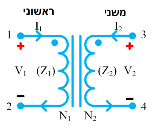
Bidirectional Coupler Characteristics
We have chosen bidirectional couplers to expose each of the four ports so that our evaluation of the shielding integrity of the packaging is comprehensive. It is worthwhile to perform a cursory review of the fundamental directional coupler parameters and their relationships.

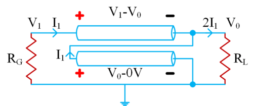
Performance characteristics of the bidirectional coupler in Figure 1 are listed below:
- Coupling value (C), or simply coupling, is the magnitude of the input power (P1) relative to the power at the forward coupled port. C = 10 log (P1/P3) dB
- Directivity (D) quantifies the ability of the coupler to distinguish between signals propagating in the forward and reverse directions at the forward coupled (P3) and reverse coupled (P4) ports.
D = 10 log (P3/P4) dB. Also, D (dB) = – 10 log (P1/P3) dB + 10 log (P1/P4) dB = I (dB) – C (dB)
- Isolation (I) is the input power (P1) relative to the power delivered to the reverse coupled port (P4). I = 10 log (P1/P4) dB
- Insertion loss (L) is the input power (P1) relative to the output power delivered to port (P2).
L = 10 log (P1/P2) dB
As with any bidirectional coupler, it is critical that the forward and reverse coupled ports be well-matched, since all four ports are brought out of the package and made available to the designer. The bidirectional coupler is symmetric, allowing it to be utilized in either direction.
Use Case 1: RF Shielding for a High-Power Core & Wire Bidirectional Coupler
The SYBDC-20-61WHP+, shown mounted to the PC board on the left side of Figure 2a, is a wideband, 20 dB bidirectional coupler constructed from a ferrite binocular core and magnet wire. One of the advantages of the core and wire construction is its ability to achieve flat coupling response over extremely wide fractional bandwidths. This component spans multiple decades (200 kHz to 60 MHz) operating across MF, HF, and even into the lower VHF range. For this style coupler, the ferrite core size and permeability are utilized for low frequency response, or to “carry the low end”. At higher frequencies, the insertion loss increases since interwinding capacitance, leakage inductance, core loss and copper loss all increase.
The RF fields associated with core & wire couplers are theoretically confined to the ferrite core and form circular flux loops around the wire. At or near the outer edges of the core, however, some of those flux loops extend around both core apertures such that some of the flux in the left aperture fringes into the right-hand side. Outside the core, there is also some flux, out to infinity in fact. This flux is much weaker due to the low permeability of air vs. the ferrite core, and due to the longer pathlength that the flux loops must traverse. Despite their relative weakness, the magnetic flux outside the core is quite capable of coupling into adjacent circuitry or even into the coupled ports due to what is known as cross-coupling, since they share the same magnetic circuit. Any cross-coupled energy can compromise coupler directivity. RF shielding is an effective method to mitigate the effects of these external electromagnetic fields in the core & wire coupler.
At a glance, it may seem that a 0.2 to 60 MHz coupler would not constitute a significant problem with radiated signals. Several factors contradict this perspective, though. The HF and VHF bands have long been used for communications due in large part to the fact that they support such efficient transmission through air. Additionally, one may consider the fact that DC-DC converter switching spikes on a PCB, which have strong content in the 30 MHz frequency range, tend to propagate very easily to adjacent circuitry and radiate effectively into an oscilloscope probe as well.
The best possible shielding of any RF component begins with ground. In the absence of excellent grounding, the degree to which a circuit or component can be shielded will be limited. We have modeled our PC boards in the following example after our test boards, and included an aluminum baseplate, to ensure that grounding performance is strong. What comes next is to hollow out a pattern in the lid to shroud the component. The pattern shown on the lid on the righthand side of Figure 2a does just that.

The main cavity is of course designed to clear the component itself. The narrow passageways, often referred to as “mouseholes”, shroud the microstrip or coplanar waveguide traces and prevent radiation into or interference from the surrounding circuity. The most notable feature perhaps is the RF gasketing. Most often, conductive silicone elastomers are deposited as long, narrow strips to shield or seal off RF from radiating around the component, particularly from port-to-port, which could compromise the coupler. While there are many “tricks of the trade” involved in this style of form-in-place gasketing related to design, materials, adhesion, etc., one of the most critical aspects for the designer is to provide some kind of compression stop for the gasket material. Often, small bosses are machined into the lid to limit compression of the gasket material to manufacturers’ specifications, generally 20-30%. In the case of the lid in Figure 2a, a groove is machined into the lid into which the elastomeric bead is deposited. The groove is larger, either in width, depth, or both, than the bead cross sectional diameter, enabling the elastomer to expand as the lid is screwed down. An X-ray view of the lid fastened to the PCB/baseplate is shown in Figure 2b.

Notice that the cavity fits tightly around the edges of the SYBDC-20-61WHP+ PC board, on which the coupler itself is mounted. It is important to have a relatively close fit since the coupler can support up to 80W of RF input power and is therefore capable of inducing strong RF fields. These fields invariably exist externally to the core itself, and the tight lid cavity helps prevent them from radiating and cross-coupling to adjacent pins. Additional shielding is achieved from the way the conductive silicone elastomeric gasketing is routed along the traces, around the input and output pins on the corners of the coupler, and even outside the screw holes. Four screws are used to fasten the lid at points close to the coupler. While some shielding is always achieved through metal-to-metal contact as the gasket compresses and the lid touches the PCB ground metallization, it is often insufficient to ensure that the best possible shielding is achieved.
Use Case 2: Shielding Technique for a High-Power Stripline Bidirectional Coupler
The SCBD-10-63HP+ stripline bidirectional coupler is shown mounted to a PC board on the lefthand side of Figure 3a. This type of stripline SMT couplers is very popular throughout the RF/microwave industry, and for good reasons. Stripline transmission is often thought of as running an RF signal through a “flattened out” coaxial cable with the edges cut away. With the center conductor sandwiched between two ground planes, RF fields are confined to the substrate, and stripline construction proves very nondispersive, achieving high levels of RF shielding and isolation. Additionally, stripline directional couplers exhibit low thru-line insertion loss, very high power handling, broad bandwidths and high operating frequencies.
For all of its advantages, it is still necessary to “come out of the package” and launch the coupler signals to a transmission medium suitable for other components on the PC board, like microstrip or coplanar waveguide. This change in transmission method from stripline to a more radiative, planar method like coplanar waveguide or microstrip results in fringing fields at the discontinuities at the junction of the PC board traces and component castellations. Left in open air, some portion of these fringing fields can radiate around the coupler from pin-to-pin, compromising directivity and isolation. This effect is particularly pronounced due to the coupler’s ability to support operation up to 6 GHz.
The lid on the righthand side of Figure 3a is utilized as an RF shield to prevent cross-coupling of signals directly from one pin to another. Its characteristics are quite similar those of the lid shown in figure 2a for a core-and-wire device, only the dimensions are modified to accommodate the stripline device. Mouseholes are utilized to channel the transmission to and from the coupler (this is often referred to as “channelization”) and conductive silicone elastomeric gaskets are deposited in routed channels and compressed when the lid is installed to achieve optimal RF shielding and isolation.

A better view of this shielding methodology is shown in the Figure 3b with a transparent view of the lid installed over the PCB. Several aspects of this mechanical design ensure excellent shielding. First and foremost, the cavity in which the coupler resides is very close to the size of the coupler itself, reducing the possibility of any stray fields leading to cross-coupling. Once again, the traces conduct signals through small cavities, or mouseholes, that are supplemented by the surrounding gasketing to ensure a tight RF shield over this region of radiative signal transmission. The potential radiation due to the discontinuities at the castellations is mitigated by the horseshoe-shaped gaskets at the corner pins of the stripline package. Segments of gasketing are compressed onto the top of the stripline package, preventing fields from radiating over the top of the package to the coupled ports. Ideally, the ground metallization on top of the SCBD-10-63HP+ would be unmasked, and that conductive ground plane would be in close contact with the lid itself through the gasketing. However, the very ends of the gasket segments do contact the top of the ground castellations and are therefore at ground potential. Finally, the cover is secured with two screws located very close to the coupler package (it is assumed that other screws will be included in the greater PCB design not far from these).

Summary
Directional couplers are ubiquitous in the RF/microwave industry. Vast amounts of information can be found on the theoretical aspects of directional couplers as well as internal design techniques on line and in textbooks. It is far less common, however, to find published literature that illustrates how to shield directional couplers in a system layout for optimum performance. In this application note, we reviewed the basic characteristics that define a directional coupler and illustrated how one type of shielding technique using a tightly-machined channelized lid with form-in-place gasketing can be applied to mitigate the effects of fringing fields. This technique optimizes directional coupler performance and minimizes unwanted effects on adjacent componentry. Two examples were given, one utilizing a high-power bidirectional coupler with core & wire construction (SYBDC-20-61WHP+) and another built with stripline technology (SCBD-10-63HP+).
It cannot be said enough, but many possibilities exist for deposition of form-in-place gasketing. At times, the gasketing is not even on the lid, but on the PC board itself. Alternatively, the gasketing may not even be of the form-in-place type, but may be of the SMT variety. Sometimes, gasketing is not utilized at all, and simple fencing and sheet metal lids are employed instead. In a subsequent application note, we will study these alternate methods of shielding and review their relative merits and drawbacks.