A Primer on Quadrature Amplitude Modulation (QAM)
 1")
While other modulation schemes discussed in this blog series (pulse, frequency, amplitude, phase) date back to the early chapters of RF engineering history, quadrature amplitude modulation (QAM) was first described by C. R. Cahn in 19602 and evolved steadily over the next few decades. In the last 25 to 30 years, no modulation scheme has seen such widespread development and application as QAM. The technology has played a pivotal role in the industry’s ability to scale data speed and capacity with user demand by packing more data onto the carrier waveform and pushing a fixed channel bandwidth closer to Shannon’s limit. QAM modulation is used widely in cellular networks and backhaul, CATV networks and fixed wireless access points (802.11), and satellite communications to name a few. See Table 3 in Reference [3] for a more detailed list of applications.
In this article, we describe QAM using basic mathematics and illustrate how a QAM modulator operates. We introduce the concept of a constellation diagram and how it relates to the time domain plots for QAM modulation. A representative set of components is then utilized to design a functional QAM modulator by way of illustration. We conclude by describing how the QAM signal is demodulated at the receiver.
QAM Fundamentals
QAM, or quadrature amplitude modulation, is a way to compress vast amounts of digital information onto an RF/analog carrier capable of transmitting this information wirelessly, without consuming more bandwidth in the modulation process. More specifically, QAM encodes digital data on two carrier waves that are 90⁰ out-of-phase (also commonly said to be “in quadrature with,” or “orthogonal to,” one another). These two data + carrier waveforms are combined (summed) downstream within the modulator and transmitted over the same channel to a receiver/demodulator. Although analog data is sometimes utilized to modulate the two carrier waveforms, because of its simplicity, popularity and ubiquity in the real world, we will focus exclusively on digital QAM in this application note. Here are the salient features of digital QAM:
- The two orthogonal analog RF carriers contain digital information.
- The two carrier waveforms are superimposed with digital information by changing the amplitude of the two carriers.
- The number of discrete carrier amplitude states defines what level of “M-ary” QAM is transmitted (e.g. 2 amplitude states yields 2 bits per symbol, or 22-QAM or 4-QAM, also 4 amplitude states yields 4 bits per symbol, or 24-QAM, or 16-QAM).
- Due to its capability to transmit multiple bits per symbol over a single channel, QAM is said to have a high degree of spectral efficiency.
- A good yardstick for the evolution of M-ary QAM over time is the IEEE 802.11 standard for transmission of QAM shown in Figure 14.
 2")
Note that Wi-Fi 7, scheduled to be released in 2024, boasts 4096-QAM, a whopping 12 bits per symbol. It may soon be time to update one’s router, depending upon the bandwidth demands of their particular system. For the purposes of this application note, and to gain a clear, fundamental understanding of digital QAM, we will go back nearly 25 years in time to 802.11b and study QPSK, also known as 4-QAM.
Theory and Argand Constellation Diagrams
The concept of QAM is not a difficult one to grasp once we understand some basic background mathematics, predominantly trigonometry. We start by looking ahead at the block diagram of Figure 2, and most notably at the two carrier waveforms that are generated from what is often referred to as a local oscillator (LO).
 3")
One waveform is a sine wave and the other is a cosine wave (the same sine wave shifted -90⁰ in phase). Recall from trigonometry that sine and cosine are 90⁰ out-of-phase, such that:
cos (θ) = sin (θ-90⁰)
Therefore, the two waveforms that result from mixing (multiplying) by sine and cosine are 90⁰ out-of-phase with one another and said to be in quadrature. In fact, the upper LO signal (sine) is modulated with the in-phase (I) signal and the lower, cosine LO signal is modulated with the quadrature (Q) signal. Now that the I and Q signals are defined, let’s take a look at equation [1] for a QAM signal in general:
h(t) = Am sin (2πft + φm) [1]
where:
- Am is the amplitude during the mth symbol interval
- φm is the phase during the mth symbol interval
- f is the carrier frequency (of the sine and cosine local oscillators)
Now using the trigonometric identity sin (a + b) = sin a * cos b + cos a * sin b, we have:
h(t) = Am sin (2πft) * cos φm + Am cos (2πft) * sin φm
h(t) = (Am cos φm) * sin (2πft) + (Am sin φm) * cos (2πft) [2]
The result is equation [2] in which we have each of our carrier waveforms [sin (2πft) and cos (2πft)] factored out explicitly. Additionally, notice that neither of these carrier waveforms contains a phase shift element in the argument, unlike the sinusoid in equation [1] which has the phase term φm. Each carrier is now multiplied by an amplitude (either Am cos φm or Am sin φm). These amplitudes are the projections of the modulation points on the I and Q axes, as shown in Figure 3,5 on what is known as an Argand diagram after Jean-Robert Argand who first conceptualized this as a way of geometrically expressing complex numbers. The two carrier waveforms are multiplied (modulated) by these amplitudes and eventually combined into a single RF stream to be transmitted over the airwaves.
 4")
We begin by setting the carriers themselves equal to 1Vpk amplitude. We first imagine that in the digital domain a zero is represented by -1V and a one by 1V. Therefore, our I and Q digital data streams will each have two possible levels, ± 1V. When one of the carriers/LOs is modulated by a ±1V digital signal, either the existing phase of the carrier is maintained, if multiplied by 1V, or it is inverted, when multiplied by -1V. Inverting the signal means shifting the carrier phase by 180⁰. In light of this ± 1V digital modulation level of the I and Q signals, and looking back at the modulation characteristics in equation [2], both Am cos φm and Am sin φm are equal to ± 1V. In the Argand diagram of Figure 3, and by using the Pythagorean theorem: Am = √12 + 12 = √2 = 1.414. We will return to the Argand diagram shortly in our discussion of the constellation diagram.
4-QAM (QPSK) in the Time Domain
The block diagram of Figure 2 utilizes notional ±1V D flip-flops to produce the I and Q data streams shown. The configuration of the D flip-flops (U1 and U2 as a shift register, U3 and U4 as a latch) combine to provide the serial-to-parallel conversion that is essential for QAM, in this case, 4-QAM. It is convenient to choose a local oscillator (carrier) frequency that is both several times greater than, and an even multiple of the I and Q modulation rate, so it is easy to distinguish between the changes in phase angle that occur within the modulator. In this case, we have chosen 4 MHz as the LO frequency and 2 MHz as the clock for the serial input data. Since the serial-to-parallel converter in a 4-QAM system arranges to have 2 bits sent at a time (one on the I carrier and one on the Q carrier), a 1 MHz symbol rate clock (SymClock) is all that is needed.
D flip-flops simply pass the state of the D (data) input through to their Q output on each rising edge of the 2 MHz clock. Flip-flops U1 and U2 operate as the shift register in Figure 2, shifting the bits of the incoming serial data stream first into U1, then from U1 to U2 with each rising edge of the Clock signal. For this intermediate step, the signals have been labeled In-phase and Quadrature. Once two new bits have been shifted into U1 and U2, the 1 MHz SymClock signal (short for Symbol Clock) latches them into U3 and U4 to complete the serial to parallel conversion. The output of U3 is the I signal, and the most significant bit (MSB), and the output of U4 is the Q signal, and the least significant bit (LSB).
The waveforms shown in Figure 4 begin with an immediate rising edge of the Clock signal, which clocks a 1 (1V) from the serial data stream through to the Q1 output of U1. On the second rising edge of the Clock signal, this 1 is clocked through to the Q output of U2 (Q2) while the next serial data bit, a 0, which we’ve defined as -1V, is clocked through to the Q1 output. This 0, 1 (-1V, 1V) pair of bits is set up at D inputs D3 and D4 of U3 and U4, respectively, when the first rising edge of SymClock latches the parallel pair of bits through to outputs Q3 (I) and Q4 (Q). Once the I and Q bit pair is at the Q3 and Q4 outputs, the state of each bit dictates the phase of its respective carrier waveform through the multiplier (mixer) function, and the two phase-shifted carriers are then summed to create a single channel over which two bits-per-symbol signal transmission occurs.
As an example, to monitor this behavior all the way through to signal transmission, follow the first rising edge of the SymClock waveform vertically in Figure 4, to where -1V, 1V are clocked in for the I and Q signals. Notice first that the I signal does not change, it remains at -1V. The product of the I signal and carrier waveform is a 180⁰ phase-shifted sine wave, as it should be when sin (2πft) is multiplied by -1. In contrast to the I signal, the Q signal does experience a polarity change. On the first rising edge of SymClock, the Q signal changes from -1V to a 1V, and the product of Q and its cosine carrier waveform changes from (-1) cos (2πft) to simply cos (2πft) as shown in the figure.
Now for the magical part, when these two modulated carrier waveforms are summed, this 0, 1 pair of bits, represented by -1V, 1V, is transmitted by the single waveform at the bottom of Figure 4. The phase shift of this waveform changes from 225⁰, which is the initial condition, to 135⁰ for this first valid bit pair, or symbol that is clocked by SymClock through to the I and Q outputs to the mixers. The transmitted waveform in the bottom plot in Figure 4 shows the phase shifts that occur as each possible symbol state is achieved. The phase shifts shown are relative to a sine wave, or in other words, the in-phase carrier waveform. The peak amplitude of the transmitted (bottom) waveform in Figure 4 is as we previously discussed, √2V.
 5")
 6")
 7")
 8")
 9")
 10")
 11")
Notice the reappearance of the Argand diagram in Figure 4. It serves as a convenient way to represent the 4 possible states of 4-QAM (or even the m possible states for m-ary QAM). Often times the state 0,0 is shown in the first quadrant of the Argand diagram. In our case, multiplication of the carrier waveforms by -1 for a bit value of 0 essentially rotates 0,0 into the 3rd quadrant, and all the other states with it. It is possible, but unnecessary (and seemingly unnatural) to define the carrier waveforms as -sin (2πft) and -cos (2πft) so that 0,0 appears in the first quadrant. Another Argand diagram is shown in Figure 5, and in this instance for 16-QAM. The diagrams of Figures 4 and 5 are more commonly referred to as constellation diagrams. For 16-QAM, note that 24 or 16 different amplitude and phase levels exist.
 12")
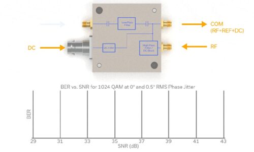
16-QAM transmits 4 bits-per-symbol, and is consequently a more spectrally efficient method of transmission than 4-QAM. The main drawback to increasing the number of bits-per-symbol is that a higher signal-to-noise ratio is required to maintain an equivalent bit error rate (BER).
A Simple QAM Modulator Signal Chain
QAM modulators are ubiquitous in this day and age, and a lot of them are baked right into the Silicon of which many an IC is comprised. To demonstrate how an actual circuit might operate, and in keeping with our IEEE 802.11 theme, we choose 2.4 GHz as our carrier frequency. The block diagram of Figure 6 considers valid I and Q inputs to the two SIM-83LH+ mixers as the starting point. I and Q data streams are applied to the IF port of the SIM-83LH+ mixers, which operate from DC-3000 MHz.
 13")
The ROS-2490C+ Voltage-Controlled Oscillator (VCO) (which would need to be phase-locked, of course) is chosen to provide the two LO (carrier) signals into the mixers. Mini-Circuits provides synthesizers with the PLL integrated onto the circuit board as well as discrete VCOs. The ROS-2490C+ VCO output is filtered by the XBF-282+ reflectionless bandpass filter. This is the perfect way to filter the oscillator so that harmonics and spurs are absorbed in the filter and not reflected back into the VCO where they can intermodulate with the carrier and other spurious outputs. The 90⁰ phase shift for the two LO inputs to the mixers is established by splitting the ROS-2490C+ output two ways using the QCN-27D+ quadrature splitter/combiner. Finally, the I and the Q-modulated carrier waveforms are summed utilizing the SCG-2-322+ in-phase, Wilkinson combiner. While perhaps not the most practical QAM modulator, the phase shift behavior of each of these notional components is more than up to the task, including the 90⁰ quadrature splitter and the 0⁰ Wilkinson combiner.
Demodulation at the Receiver End
On the receive side of QAM, imagine for the moment that the summing function or combiner at the output of the transmitter in Figure 2 is actually the input, and the component functions as a splitter, yielding two identical RF-modulated QAM data streams. Demodulation then proceeds from right-to-left (backwards) in Figure 2 by mixing each of these two identical, modulated data streams with a replica of each of the orthogonal LO signals from the original transmission, separating I and Q into their constituent baseband digital data streams. A multitude of digital reformatting of the data can occur at this stage (at baseband). The essence of QAM reception and demodulation may be visualized as the mirror image of the original transmission, or that process in reverse. This is, of course an oversimplification because we have assumed that the orthogonal clock signals that perform the demodulation are somehow synchronized with those at the remotely-located receiver, or that that receiver has some a priori knowledge of the exact phase of the LOs and the clock(s). In reality, synchronization is accomplished by transmitting something along with the data, or a specific data pattern that the receiver knows to recognize as the sync signal.
Summary
In this application note, we detail a serial-to-parallel converter that yields I and Q data for QAM modulation of two carrier waveforms. We study the basic mathematics behind QAM, and illustrate how a QAM modulator operates through a series of digital timing diagrams including sinusoidal plots. We relate the constellation diagram to these time domain plots for QAM modulation, as well as introduce the constellation diagram for 16-QAM. A set of real components is designed to illustrate a functional, albeit notional QAM modulator circuit.
References:
- Did Gomer Pyle say ”Shazam!” because of the comic book character? Probably, yeah. (metv.com)
- IRE Transactions on Communications Systems ( Volume: 8, Issue: 3, September 1960 pp 150-155) “Combined Digital Phase and Amplitude Modulation Communication Systems” C. Cahn https://doi.org/10.1109/TCOM.1960.1097623
- IEEE Xplore Full-Text PDF:
- Understanding the Wi-Fi® Variants – Tech Briefs
- I/Q Signals 101: Neither Complex Nor Complicated | Wireless Pi