A Primer on RF Semiconductors (MMICs)
Radhakrishna Setty, Technical Advisor
Introduction
Semiconductors are ubiquitous in modern society. In addition to microprocessors for computing technologies, they are used in practically every active wireless communications system including cell phone towers, cell phones, radars and satellites to name a few. Mini-Circuits designs and produces several semiconductor-based (MMIC) components used in many of these applications. This article explores the fundamentals of RF semiconductors to provide a foundational understanding of how they function, starting from atoms.
Atoms
The smallest particle of matter that retains the properties of the matter is called an Atom, derived from the Greek word atomos which translates loosely to “uncuttable” or “indivisible.” An atom consists of a nucleus with positively charged protons plus neutral neutrons, and negatively charged electrons. Protons have approximately 2000 times the mass of electrons and are relatively immobile.
The famous physicist, Niels Bohr (1885-1962) made an intuitive suggestion that electrons must occupy certain orbits, and that their energy depends on distance from the nucleus. This implies that electrons can only have certain fixed or “quantized” energies. The energy required to remove an electron from an atom is called an ionization potential. The farther away an electron is from the nucleus, the easier it is to remove, and the lower its ionization potential. The energy associated with an electron is so small, it is common practice in the industry (and in this article) to use electron volts (eV) as a standard unit, where:
1 eV = 1.6 x 10⁻¹⁹ Joules.
If an electron falls through a potential of 1V, its kinetic energy increases and potential energy decreases by 1eV. The charge of an electron is e=1.6 x 10⁻¹⁹ Coulombs (C). Stated another way, the number of electrons per one Coulomb is about 6 x 10¹⁸. One Ampere of current through a circuit is 1 Coulomb/sec which works out to about 6 x 10¹⁸ electrons per second. At a smaller scale, 1nA (10-9 A) is the flow of about 6 x 10⁹ electrons per second, what seems like a paradoxically large number for such a small current!
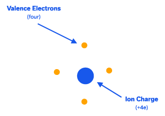
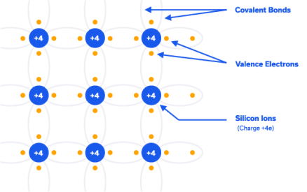
Silicon, one of the most popular semiconductors has 14 electrons. All but 4 electrons in its outer shell are tightly bound to the nucleus, and a silicon atom can be pictured as an ion of charge +4e surrounded by 4 electrons, called valence electrons, which are available for bonding. In a silicon crystal, these 4 electrons are shared with adjacent atoms in covalent bonds.
A simplified 2-dimensional picture of a silicon crystal is shown in Figure 2. At extremely low temperatures (0K) all the valence electrons are bound one atom to the next, and none are available for conduction so silicon behaves like an insulator (more on this below). As the temperature rises, thermal energy is supplied to the crystal and some of the bonds are broken, leaving some electrons available for conduction. In other words, silicon behaves like a conductor under some conditions and an insulator under others. This property is what classifies it as a semiconductor. Let us delve deeper into this topic.
Band Gap Theory
According to Pauli’s exclusion principle (1925), no two electrons can have same quantum state. Simply stated, energy levels of valence electrons in a silicon crystal are discrete, distinct and close together, and intuitively it is convenient to think of each energy level as a band (Figure 3), which we will call the valence band. The energy levels of free electrons participating in conduction fall within the conduction band. Valence electrons do not participate in conduction unless an energy equal to the band gap between the valence band and conduction band is supplied, for example by heat or light. In silicon, the band gap is 1.12eV. By comparison, metals have no band gap, and in insulators it is arbitrarily defined as greater than 3 to 4eV.
Intrinsic and Extrinsic Semiconductors
As stated before, in silicon crystal, at extremely low temperatures, all the valence electrons are bound one atom to the next, and none are available for conduction, so it behaves like an insulator.
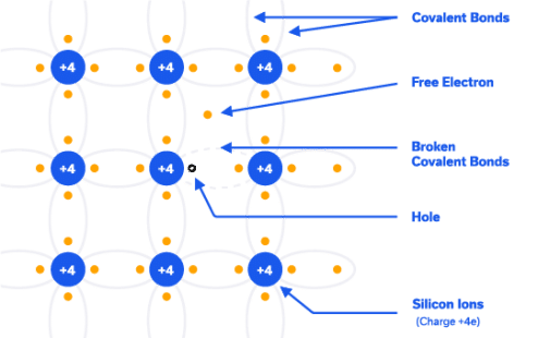
As temperature increases (even at room temperature) some bonds are broken creating electron hole pairs, and these are available for conduction. Hence the name semiconductor. Pure silicon is called an intrinsic semiconductor.
At room temperature, T=~300K, energy is kBT, where kB is Boltzmann’s constant
kB= 8.617 x 10⁻⁵ eV/K
Therefore kBT= 8.617 x 10-5 x 300 = 0.025V eV
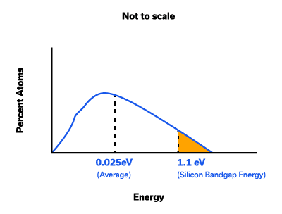
The question is, how can such a small thermal energy enable some valence electrons to jump a band gap of 1.12eV? Not all electrons are at the same temperature, 300K is an average temperature. The Maxwell-Boltzmann distribution (Figure 4) shows that a small fraction of electrons has energy in excess of the band gap energy and are available for conduction at room temperature, represented by the shaded area in the figure.
The number of electrons available for conduction in pure silicon at room temperature is so small, it is not of much use. For example, the voltage required for 1µA current across a 3mm long crystal with a cross section of 50µm x 100 µm is 1.38kV, which too high. Comparing it to metal, silicon has free electrons of 1.5 x 10¹⁰/cm3 at room temperature vs. 1028/cm3 in metal, many orders of magnitude lower.
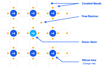

N-Type Extrinsic Silicon: By “doping” the silicon crystal with atoms having five valence electrons (pentavalent), an excess electron is made available for conduction (Figure 6). Pentavalent atoms include antimony, phosphorus and arsenic and are called donor impurity atoms as they donate an excess electron which is loosely bound, and can be easily promoted into the conduction band. See the band diagram in Figure 7.
By doping as little 1 donor atom per 108 silicon atoms, the voltage required to draw 1µA current in the cross section mentioned above drops to 0.05V.
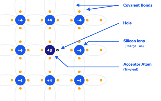
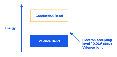
P-Type Extrinsic Silicon: On the other hand, by doping the silicon crystal with atoms having three valence electrons (trivalent/acceptor), an excess hole is made available for conduction. Trivalent atoms commonly used are group 3 atoms in the periodic table, such as Boron. In terms of the band diagram, this creates an energy level just above valence band allowing valence electrons to jump to that band, creating holes in the valence band. Majority charge carries are holes in P-Type Silicon.
For manufacturability purposes, all the components (transistors, diodes, resistors etc.) should be formed on a planar wafer. For example, to create a P-N junction, by doping a P-type semiconductor substrate at select locations with excess donor atoms (over and above acceptor atoms), N-type regions can be created. This is the key property is used in monolithic circuits as shown in Figure 10.

Similarly, by doping an N-type semiconductor at select locations with excess acceptor atoms, P-type regions can be created.
Compound Semiconductors
Silicon (and Germanium) belong to Group 4 in the periodic Table and have four valence electrons. Compound semiconductors can be formed by combining Group 3 (three valence electrons) and Group 5 (five valence electrons) resulting in an average of 4 valence electrons per atom. Examples are compounds of Ga (Gallium) and As (Arsenic) to form GaAs, which Mini-Circuits uses in many of our MMIC products. A slight increase in the proportion of As produces n-type doping, and a slight increase in the proportion of Ga produces p-type doping. The higher mobility of electrons in GaAs (compared to silicon) enables it to be used in high-frequency circuits. The higher bandgap of GaN enables it to be used in power amplifiers delivering higher power than Si or GaAs. Some of the properties of popular RF semiconductors are summarized in Table 1. Note, the cost of all semiconductor materials is not same. In increasing order of cost, the material ranking goes Silicon, GaAs and GaN.

Mobility is defined as the ratio of drift velocity to electric field intensity. In direct bandgap materials, valence band maxima and conduction band minima occur at the same momentum. In indirect bandgap materials, it occurs at different momentums. This concept will be discussed further in subsequent articles.
Metal-Semiconductor Junctions
To make an electrical connection to a semiconductor, a bond wire (metal) needs to be attached. It is interesting to note that some metals create an ohmic contact and others create a rectifying junction. Both types of contacts are useful. The later is also called Schottky Barrier junction. In order to understand metal-semiconductor junctions, one needs to define a work function (Albert Einstein won a Nobel prize for this in 1921). The work function of a material is the energy required to remove an electron from the level of the chemical potential and give it enough energy to escape to infinity and arrive there with zero energy3, defined by symbol Фm and Фs for metal and semiconductor, respectively.
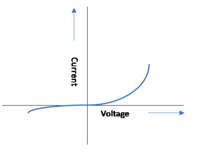
Фm > Фs for type-N semiconductors, and the resulting junction is rectifying, which means current is allowed to flow in one direction. Such contacts are also called Schottky barrier contacts, and are used extensively in frequency mixers, as they are fast switching. The V-I characteristic of a Schottky Barrier diode is shown in Figure 11.
P-N Junctions
Rectifying junctions can also be formed using P-N junctions, where N-Type and P-type materials are combined, and the crystal structure is continuous, as in Figure 12. Electrons flow from N-type to P-type and holes from P-type to N-type. This forms a barrier to potential, and at equilibrium, there is no current flow. By connecting an N-type material to the negative terminal of a battery and a P-type material to positive, the barrier to flow is lowered and current starts flowing. If an N-type material is connected to the positive terminal of a battery and P-type is connected to the negative terminal, barrier potential increases, the junction is reverse biased, and very little current flows. The resulting V-I curve is very similar to that shown in Figure 11. P-N junctions are very slow switching and are not of much use at RF/Microwave frequencies.

Summary
We’ve covered the basics of semiconductors together with Ohmic and rectifying contacts and P-N junctions. Extensive tutorial treatments of the each of these topics topics can be found in the references cited below. Advanced topics such as HBTs, PHEMTs, GaN will discussed in future articles in this series.
References:
- Maitland Jones Jr., “Organic Chemistry”, 2005, W.W. Norton & Company
- William Shockley, “Electrons and Holes in Semiconductors”, D.Van Nostrand Company Inc., 1959
- University of Cambridge TLP Library, Introduction to Semiconductors
- MIT, OpenCourseWare Search (mit.edu)
- Paul A. Tipler, Gene Mosca, “Physics for Scientists and Engineers- Vol 1”, W.H.Freedman and company, 2004
- Jacob Millman & Arvin Grabel, “Microelectronics” McGraw-Hill International, 1988
- Khan Academy, Semiconductors | Class 12 Physics (India) | Science | Khan Academy


