Product Highlight: ZVE 18GB+ Wideband RF Low Noise Amplifier (LNA) with High Linear Output Power
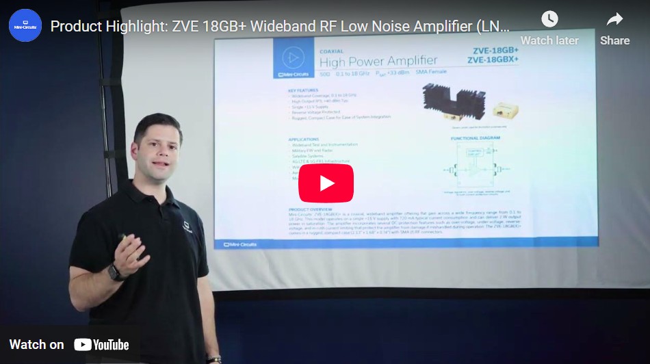
Mini-Circuits’ High-Frequency Product Line Engineering Manager, Dan Ford explains the unique features of the ZVE-18GB+ wideband low noise amplifier (LNA) operating from 0.1 to 18 GHz. This model was designed for modern RF systems requiring high linear output power and low noise performance for improved system signal-to-noise ratio (SNR). Operating on a single +15V supply with built-in DC protection features, the amplifier achieves flat gain of ~30 dB across its full bandwidth, greater than 1W output power at 1 dB compression (greater than 2W at saturation), and +40 dBm OIP3.
Understanding Additive Phase Noise in RF & Microwave Amplifiers – Part 4
Mini-Circuits R&D Fellow, Joe Merenda recently presented a tutorial on Amplifier Additive Phase Noise at the 2025 Low-Level Radio Frequency Workshop at the Thomas Jefferson National Accelerator Facility in Newport News, VA. In this fourth episode of our Additive Phase Noise series, he shares this tutorial for the benefit of the broader RF and microwave engineering community. In this session, Joe explains the measurement setup and reviews fundamentals of additive phase noise theory. He then discusses differences between small signal and large signal behavior and the effect of AM-PM distortion on APN performance. The tutorial concludes with practical cases of additive phase noise performance in various cascade design examples.
Outstanding OIP2 from a Small Dual MMIC Amplifier

Remarkably, the concept of the push-pull connection spans three centuries. William W. Dean of the Bell Telephone Company of Missouri first described the push-pull-connected telephone transmitter in Patent No. 549,477, dated November 5, 1895.1 Next, Sir John Ambrose Fleming invented the first vacuum tube in 19042 and while Lee De Forest added the grid to Fleming’s “valve” in 1906, calling it the “audion,” it was Fritz Lowenstein in his April 24, 1912 patent application who first discovered that applying a negative bias to the grid of De Forest’s tube turned it into an audio amplifier.
Edwin Henry Colpitts of the Western Electric Company was awarded Patent No. 1,128,292, for an “electric wave amplifier” on February 16, 1915, which covered the push-pull circuit by connecting two vacuum tubes like De Forest’s audions like a primitive precursor to the transistor.3,4 Over a hundred years ago, Colpitts recognized that “a certain amount of distortion in the output waves is avoided”3 by utilizing this configuration.
Anatomy of a 37-40 GHz 5G n260 Band Front-End with a Discrete LO

The appetite for greater download speeds and lower latency amongst modern mobile device users can be satisfied by higher RF bandwidths. The greatest bandwidths available are found in the mmWave bands, such as 5G band n260 (often referred to as the 39 GHz band, or upper Ka band) which spans 37 to 40 GHz. Although signals in the mmWave band region have the shortest range and poorest ability to penetrate obstacles like buildings and irregular terrain, they do afford the opportunity to achieve incredibly high data rates. Devices capable of receiving the 5G n260 band are theoretically capable of achieving download speeds of up to 20 Gbps under ideal conditions, such as over a short range (< 500 meters) and for line-of-sight transmission. Under real-world conditions, one of the major telecommunications network operators has deployed a 5G FR2 n260 band solution that offers speeds up to 3 Gbps1, and every one of the top three operators has deployed n2601, predominantly where dense wireless traffic is located – stadiums, convention centers, large urban areas, etc.
How to Build a High-Performance SSB Upconverter

Upconverters are ubiquitous in modern RF systems, translating everything from baseband quadrature DDS signals to many of today’s mmWave signals. An X-band upconverter with sideband suppression utilizing an IQ mixer is prototyped in this article to enable the reader to better understand the up-conversion process and the mathematics behind sideband suppression itself.
While integrated forms of upconverters are widely available for many applications, it is interesting to construct a modular upconverter with a significant number of Mini-Circuits’ parts to see how the components interact and how each contributes to overall system performance. Filtering, frequency multiplication, amplification, signals in quadrature, and sideband suppression are a few of the concepts covered when reviewing the system architecture. Finally, we discuss use cases where up-conversion combined with sideband suppression is essential for achieving RF system performance goals.
Understanding Additive Phase Noise in RF & Microwave Amplifiers – Part 3

In the 3rd and final part of our series on amplifier additive phase noise testing at Mini-Circuits, we continue our investigation into cascaded amplifiers. Part 2 considered two identical amplifiers in series and four identical amplifiers in parallel. However, we were unable to clearly demonstrate the improvement in 1/f noise provided by the parallel configuration due to equipment noise floor limitations.
In Part 3 we address this limitation by driving the four parallel amplifiers with a single amplifier, all identical, and demonstrate that the cascaded performance is dominated by the single driver amplifier.
We also describe how to best optimize the input power levels into each amplifier in order to avoid regions of high AM-to-PM distortion and achieve optimum performance over a wide bandwidth.
About Mini-Circuits:
Mini-Circuits is the world’s preferred supplier of RF and microwave components and systems. With 14 design, manufacturing and sales locations in nine countries, as well as hundreds of sales channel partners worldwide, Mini-Circuits offers 27 product lines comprising over 10,000 active models. Over 20,000 customers choose Mini-Circuits for the demanding quality standards, world-class customer support, on-time delivery and value pricing that have earned the industry’s trust for over 50 years.
Understanding Additive Phase Noise in RF & Microwave Amplifiers – Part 2

In this second video in our series on RF amplifier additive phase noise, Mini-Circuits VP of engineering, Joe Merenda takes a deeper dive into cascaded amplifiers in LO chains. The discussion explores how to configure lineups of 2 amplifiers in series, and 4 amplifiers in parallel to achieve optimum additive phase noise performance. Testing phase noise in cascade vs. parallel setups, observing noise performance across amplifiers, and characterizing behavior in high-frequency environments are discussed in turn.
About Mini-Circuits:
Mini-Circuits is the world’s preferred supplier of RF and microwave components and systems. With 14 design, manufacturing and sales locations in nine countries, as well as hundreds of sales channel partners worldwide, Mini-Circuits offers 27 product lines comprising over 10,000 active models. Over 20,000 customers choose Mini-Circuits for the demanding quality standards, world-class customer support, on-time delivery and value pricing that have earned the industry’s trust for over 50 years.
Understanding Additive Phase Noise in RF & Microwave Amplifiers – Part 1
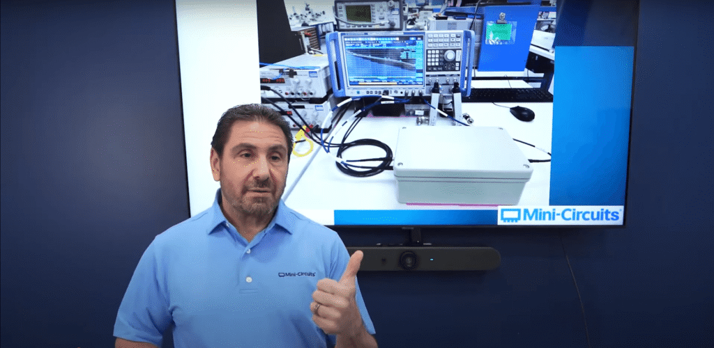
The webinar “Understanding Additive Phase Noise in RF & Microwave Amplifiers – Part 1” features Joe Merenda, Vice President of Engineering at Mini-Circuits, presenting an in-depth overview of additive phase noise (APN) in RF and microwave amplifier systems. Additive phase noise refers to the additional phase noise that an amplifier introduces to an already modulated input signal. This concept is especially important in high-frequency applications such as radar, satellite communication, and wireless systems where phase purity directly affects system performance.
RF Amplifier and Filter Testing with Mini-Circuits Power Sensors
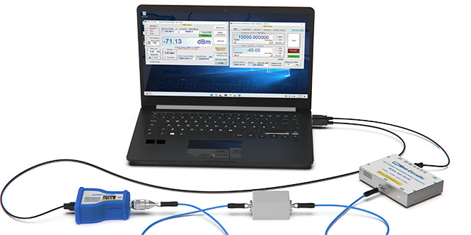
RF Amplifier and Filter Testing with Mini-Circuits Power Sensors Introduction When measuring common RF components, such as filters and amplifiers, RF power sensors provide an accurate, cost-effective way to obtain meaningful data. For RF filters, parameters such as insertion loss, return loss and desired frequency response (passband and stopband) should be considered. For RF amplifiers, […]
Wideband Amplifiers – Variable and Temperature-Compensated Gain
Wideband Amplifiers – Variable and Temperature-Compensated Gain
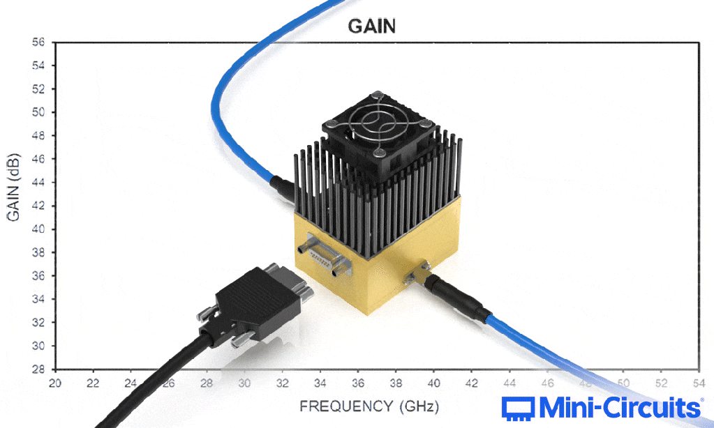
Many types of RF systems and applications that span from the upper end of microwave frequencies to the lower end of mmWave have arisen in recent years. Meeting system requirements over such a wide bandwidth and high frequency range, or even a broad sub-band requires that system performance parameters be stable, and the parameter that most often concerns microwave/mmWave system designers is gain. Mini-Circuits addresses these concerns with two amplifier types from our ZVA-series of wideband microwave/mmWave amplifiers that equip the system designer with either variable gain, or temperature-compensated, stable gain. Not only can gain be temperature-stable or variable, but at approximately 50 dB, it is also plentiful. Combine this with a low NF, high linearity and interactive telemetry, and Mini-Circuits’ wideband, variable and temperature-compensated gain amplifiers prove to be one of the highest-performing and most flexible amplifier solutions on the market today. Read on to find out how adjustable or temperature-stable gain and the ability to monitor output power can be beneficial when it comes to designing a system for any one of a number of applications.


