Understanding Additive Phase Noise in RF & Microwave Amplifiers – Part 2

In this second video in our series on RF amplifier additive phase noise, Mini-Circuits VP of engineering, Joe Merenda takes a deeper dive into cascaded amplifiers in LO chains. The discussion explores how to configure lineups of 2 amplifiers in series, and 4 amplifiers in parallel to achieve optimum additive phase noise performance. Testing phase noise in cascade vs. parallel setups, observing noise performance across amplifiers, and characterizing behavior in high-frequency environments are discussed in turn.
About Mini-Circuits:
Mini-Circuits is the world’s preferred supplier of RF and microwave components and systems. With 14 design, manufacturing and sales locations in nine countries, as well as hundreds of sales channel partners worldwide, Mini-Circuits offers 27 product lines comprising over 10,000 active models. Over 20,000 customers choose Mini-Circuits for the demanding quality standards, world-class customer support, on-time delivery and value pricing that have earned the industry’s trust for over 50 years.
Understanding Additive Phase Noise in RF & Microwave Amplifiers – Part 1
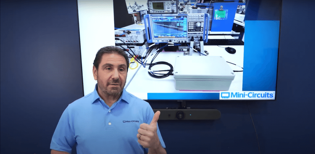
The webinar “Understanding Additive Phase Noise in RF & Microwave Amplifiers – Part 1” features Joe Merenda, Vice President of Engineering at Mini-Circuits, presenting an in-depth overview of additive phase noise (APN) in RF and microwave amplifier systems. Additive phase noise refers to the additional phase noise that an amplifier introduces to an already modulated input signal. This concept is especially important in high-frequency applications such as radar, satellite communication, and wireless systems where phase purity directly affects system performance.
Care & Handling of RF/Microwave Adapters
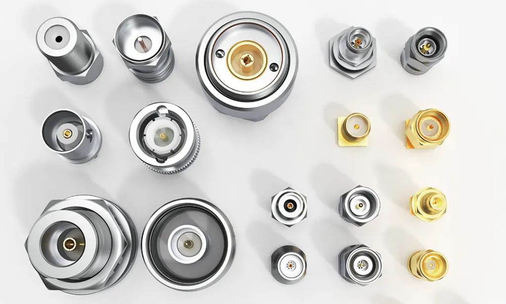
The performance of every RF system depends on the quality and application of each component. In industry, much of the focus is on complex, expensive RF equipment. At the same time, it is also prudent to give equal attention to the quality and type of interconnections between components.
RF cables, connectors, adapters, and accessories (for the purposes of this paper, this family of components will be referred to as RF connectors) directly impact system performance. Impedance mismatch, insertion loss, and return loss are just a few of the parameters that impact the reliability, repeatability and accuracy of an RF system. This paper will focus mainly on coaxial connectors — by far the most common type of interconnect. Still, the principles discussed apply to a range of connectors and interconnections.
Measuring Wideband RF Signals with Power Sensors Fundamentals
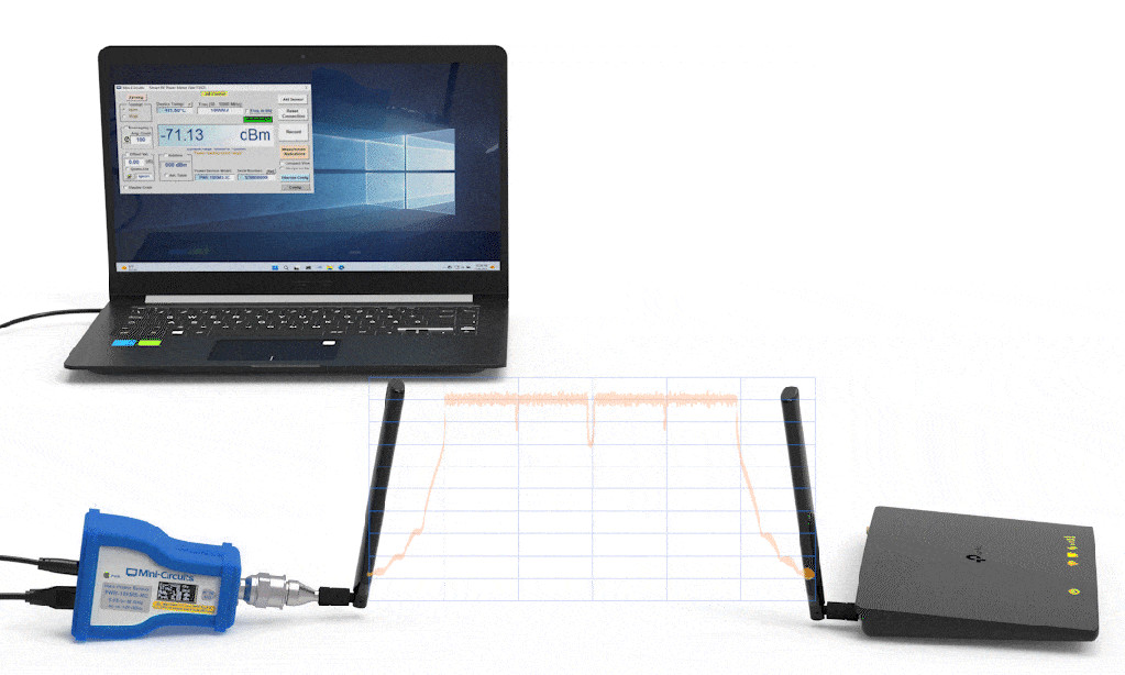
The ongoing drive to transmit and receive more information wirelessly in a given bandwidth forces modern RF systems to continually increase their spectral efficiency. Some of the earliest commercial wireless systems from several decades ago utilized channel bandwidths of a just few kHz. With more and more pressure being placed on wireless systems, everything from Bluetooth headsets to aviation infrastructure to self-driving cars require wider bandwidths to achieve the required data throughput, with signal bandwidths approaching 1 GHz or more.
In aerospace/defense applications, wider RF signal bandwidths not only provide more capacity for voice and data, but their wider bandwidths also make jamming and countermeasures more difficult. One popular technique is spread spectrum, a technique in which a wide bandwidth signal is created that operates well in a noisy environment. Spread spectrum was originally adopted by the cellular industry as traditional 2G Code Division Multiple Access (IS-95 CDMA, for example) and evolved to 3G W-CDMA, with signal bandwidths approaching 5 MHz per channel.
Increasing the RF system bandwidth is one way to accommodate larger amounts of data throughput. Various modulation techniques, encoding and frequency and time division multiplexing are a few ways in which increases in spectral efficiency can be achieved. Invariably, wider bandwidths are implemented as part of an overall strategy to transmit and receive more information. Accurately measuring the power of wideband RF signals ensures efficient power usage as well as high signal quality.
How To: Measuring Pulsed RF Power
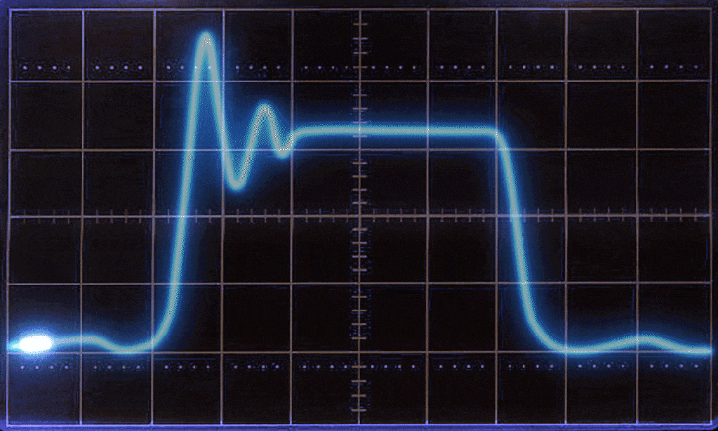
Power is a necessary parameter to measure across a wide range of modern applications and there are an assortment of instruments and methods for measuring it. Best practices, such as high-quality connectors and properly torqued components from Mini-Circuits can help minimize errors in any RF measurement. With high-performance test systems, the user should take great care to understand ways of minimizing any source of measurement error.
For measuring RF power and other pulse-modulated RF waveform characteristics, Mini-Circuits’ RF power sensors offer the convenience of modern connectivity (USB, LAN), an interactive power GUI, exceptional accuracy, and outstanding price points compared with other types of RF instrumentation.
GaAs Switches Are a High-Performance Alternative to SOI for Test & Measurement Instrumentation
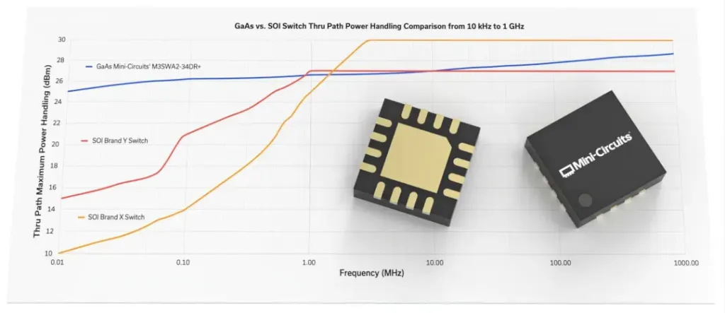
The RF switch is an important element in test & measurement instrumentation for routing signals and for filtering them, utilizing switch manifolds and filters. One unique challenge for switches in the test & measurement market is the requirement to pass relatively high-level signals of greater than +20 dBm at very low frequencies, often down to 9 kHz. It seems that 9 kHz is an unusual frequency until you consider that the frequency limits for IEC/CISPR 11, EN 55011 for conducted and radiated emissions of ISM RF equipment are 9 kHz to 400 GHz, and that prevailing test equipment must be capable of measuring to these limits. Speed, including settling time is also of paramount importance in test and measurement, especially for Automatic Test Equipment (ATE). In ATE systems, SOI switch delays that are 100 times greater than the few tens of ns exhibited by GaAs switches must often be avoided, as these delays can become cumulative throughout an instrument’s signal chain and over the course of long, complex measurement routines. The final challenge for the designer is cost containment, particularly when equipment is designed with a significant number of switches.
RF Amplifier and Filter Testing with Mini-Circuits Power Sensors
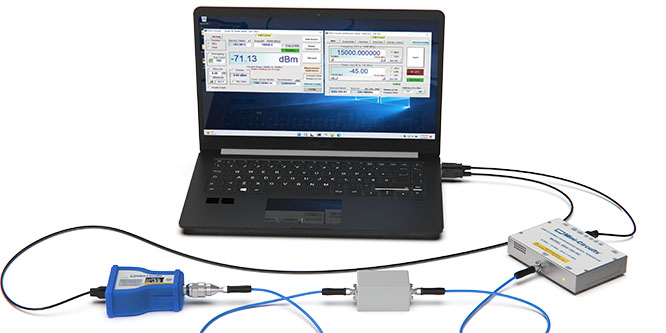
RF Amplifier and Filter Testing with Mini-Circuits Power Sensors Introduction When measuring common RF components, such as filters and amplifiers, RF power sensors provide an accurate, cost-effective way to obtain meaningful data. For RF filters, parameters such as insertion loss, return loss and desired frequency response (passband and stopband) should be considered. For RF amplifiers, […]
Wideband Amplifiers – Variable and Temperature-Compensated Gain
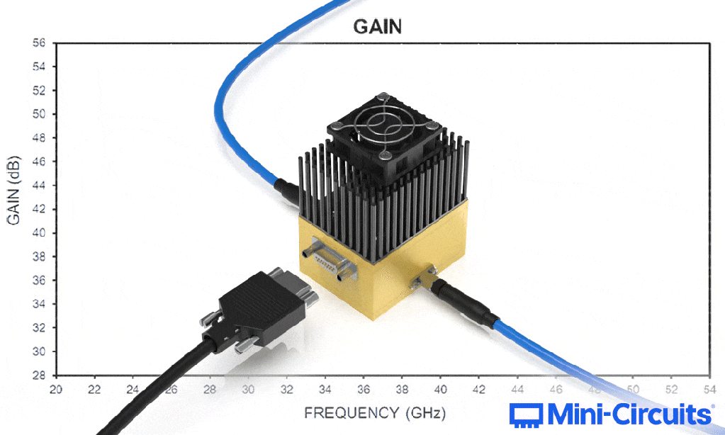
Wideband Amplifiers – Variable and Temperature-Compensated Gain
Many types of RF systems and applications that span from the upper end of microwave frequencies to the lower end of mmWave have arisen in recent years. Meeting system requirements over such a wide bandwidth and high frequency range, or even a broad sub-band requires that system performance parameters be stable, and the parameter that most often concerns microwave/mmWave system designers is gain. Mini-Circuits addresses these concerns with two amplifier types from our ZVA-series of wideband microwave/mmWave amplifiers that equip the system designer with either variable gain, or temperature-compensated, stable gain. Not only can gain be temperature-stable or variable, but at approximately 50 dB, it is also plentiful. Combine this with a low NF, high linearity and interactive telemetry, and Mini-Circuits’ wideband, variable and temperature-compensated gain amplifiers prove to be one of the highest-performing and most flexible amplifier solutions on the market today. Read on to find out how adjustable or temperature-stable gain and the ability to monitor output power can be beneficial when it comes to designing a system for any one of a number of applications.
Phase-Matched Cable Assemblies
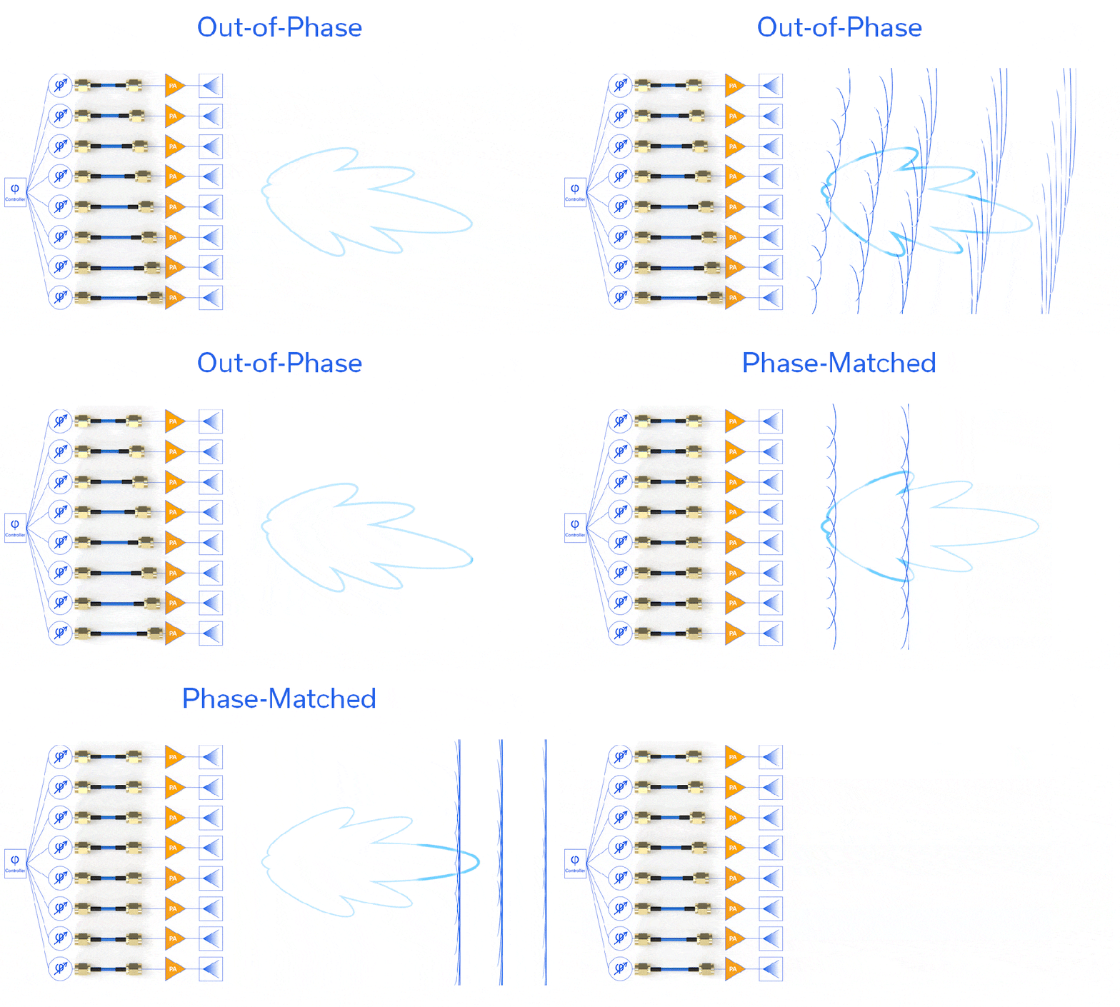
Phase-matched cable assemblies are ubiquitous, and modern-day phase matching requirements serve to drive their growing popularity. As electrical length matching requirements have tightened to less than one or two degrees, the mechanical precision with which various styles of cable are constructed has improved to keep pace. Additionally, dielectrics more exotic than tried-and-true Teflon are being researched and introduced to afford greater phase stability. Volumes have been written on how to phase-match cable assemblies and dozens and dozens of companies practice this discipline. Why is phase-matching so prevalent, and why does it matter so much? In this article we answer these questions by highlighting many phase-matched cable applications and the effect of varying phase length on systems in the RF/microwave domain. We also describe Mini-Circuits’ capabilities in the phase-matching cable arena.
A Dual Band Channel Sounder Module for FR1 & FR3 Band Modelling (6.75 GHz & 16.95 GHz)
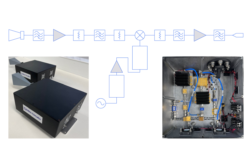
While much research has been devoted to exploring millimeter-wave bandwidths for high-data-rate wireless communications, much of the deployment of 5G to date has relied on frequencies in the sub-6 GHz (FR1) region of the spectrum. The channel capacity of the FR2 bands has been used in urban environments with high subscriber demand where infrastructure can be installed with sufficient density to compensate for the short range and poor penetration of high-frequency signals. Meanwhile, network operators still rely on lower-frequency signals for more ubiquitous coverage.
Similar desire for the data capacity and speed of millimeter-wave and sub-THz transmissions with broad network coverage and low power requirements of lower frequencies has spurred strong interest in the FR3 bands (7 to 24 GHz) as a possible “Goldilocks zone” for the next phases of 5G and 6G development.
Professor Ted Rappaport and his graduate research fellows of NYU WIRELESS in Brooklyn, New York are among the leading researchers exploring the propagation characteristics of 5G and 6G frequency bands under consideration for commercial use by the ITU and telecom industry. In 2022 Rappaport and his team visited Mini-Circuits’ facilities in Brooklyn, and Deer Park on Long Island as a test bed for their work to develop the first spatial statistical model for ultra-wideband signals above 100 GHz in a real-world factory environment.


