MMIC Technologies: Pseudomorphic High Electron Mobility Transistor (pHEMT)
Radha Setty, Technical Advisor
Introduction
Pseudomorphic High-Electron-Mobility-Transistor (pHEMT) is one technology Monolithic Microwave Integrated Circuit (MMIC) designers and fabs use to develop and manufacture microwave integrated circuits. pHEMT has gained popularity as a building block of many MMICs produced by electronics manufacturers like Mini-Circuits due to its superior wideband performance characteristics including low noise figure, high OIP3 and excellent reliability up to 40 GHz and beyond. pHEMT uses heterojunctions between semiconductors of different compositions and bandgaps to achieve outstanding high-frequency performance. This article delves into the physics of pHEMT operation, advantage, and reliability test results. A link to a summary of Mini-Circuits’ pHEMT products is also provided.
Field Effect Transistor (FET) Family [1]
In its most simplistic form, a Field Effect Transistor (FET) consists of three terminals: source, drain and gate, as shown in Figure 1. The flow of carriers (electrons/holes) from source to drain is controlled by the electric field applied to the gate, hence the name Field Effect Transistor.

In real-world practice, this simple structure extends to a whole family of devices depending on how it is implemented. This article focusses on HEMT/pHEMT.
Review: Crystal Structure, Lattice Constant and Mole Fraction [1,2]
A brief review of some basic terms will help instill an understanding of the underlying physics of HEMTs and pHEMTs.
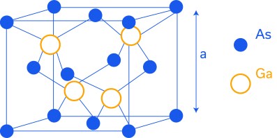
A crystal such as GaAs has a periodic placement of atoms. The smallest assembly of atoms that can be replicated to form the entire crystal is called a primitive cell. Figure 2 shows a primitive cell of GaAs. The dimension of the cube is called the Lattice Constant, “a,” usually expressed in Angstroms, Å (1Å =10-10 m) and is a function of temperature. As an example, the lattice constant of GaAs is 5.653 Å at 300K.
One way to express the relative amounts of substances in compounds is with a measure called the mole fraction. Mole fraction X is the ratio of moles of one substance in a mixture to the total number of moles of all substances. For a mixture of two substances, A and B, the mole fractions of each would be written as follows:

and

Epitaxy [1,6,14]
It is important to understand the concept of epitaxy, as most semiconductor wafer manufacturing depends on it. From the Greek roots “epi” and “taxis”, the word epitaxy means “to arrange upon.” Epitaxial growth starts with a substrate upon which a film of the same material as the substrate or a different material is grown. Epitaxy, or “epi” in industry short speak, is a unique growth mode in which the crystalline structure of the deposited film matches that of the substrate, atom for atom as the layers are deposited.
For example, the growth of AlGaAs over GaAs has to result in bonding of atoms without interface defects to be suitable for use in electronics. One such technique is Molecular Beam Epitaxy (MBE) where evaporation or sublimation of heated elements such as Al, Ga, and As results in molecular beams which impinge on heated GaAs substrate kept at very low pressure (10-5 torr). Dopants such as Si are incorporated into layers during growth. Epi growth occurs at a rate on the order of 1 atomic layer per second. One second is a relatively long time, so precise control of epi growth is possible. pHEMTS/HEMTS are fabricated on epitaxial wafers.
Band Gap Engineering
The basics of band gap theory were discussed in the previous article in this series [3]. Many exciting new innovations in electronics are made possible by band gap engineering in which compounds of various elements are formed to realize a desired band gap. Significant uses of bandgap engineered products include LEDs, Lasers, HEMT/pHEMTs, HBTs (which will be covered in an upcoming article) and many others.
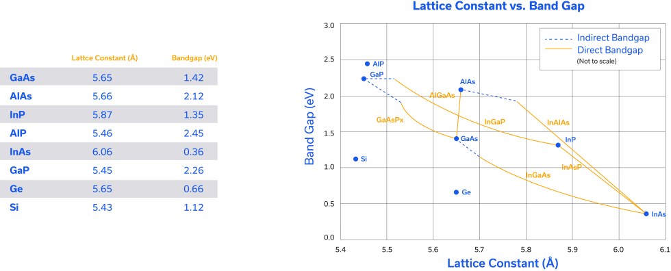
Semiconductor materials, both elemental and compound, have defined lattice constants and bandgaps [1,4,5,6]. Figure 3 shows band gap energy vs. lattice constant for various crystals such as GaAs, AlAs, InAs and others. By forming compounds of various semiconductors, the band gap can be engineered or varied to a desired value. For example, the compound of GaAs and AlAs is AlGaAs; by changing the mole fraction, various bandgaps from 1.42eV (that of GaAs) to 2.12eV (that of AlAs) can be realized. Similarly, InGaAs can have a bandgap from 0.36eV to 1.42eV depending upon the mole fraction of its constituents. Note that the lattice constants of GaAs and AlAs are very similar. Therefore, the lattice constant of AlGaAs is very similar to that of GaAs/AlAs. This is a valuable attribute when forming heterojunctions of GaAs and AlGaAs and allows epitaxial growth of thicker AlGaAs material over GaAs without creating lattice-mismatch-related defects. This is not the case for InGaAs over GaAs, as the lattice constant can change from 5.65 to 6.06Å which can create lattice mismatch and surface defects.
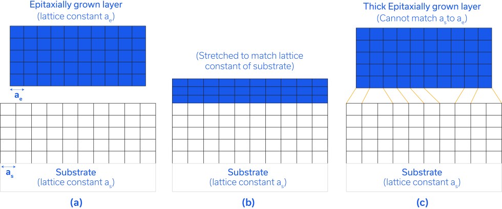
Figure 4 shows two materials with different lattice constants: as (substrate) and ae (epi-material). In Figure 4(a), the substrate and epitaxially grown layers are shown in isolation. Figure 4(b) shows a thin layer grown on the substrate. In this case, the epi material stretches to match the lattice constant of the substrate (like a thin layer of rubber which can be stretched), resulting in no broken bonds. When the epi layer is thick, it is no longer elastic (like thick rubber which cannot be stretched), resulting in broken bonds and creating undesirable defects.
If the thickness of the epi material is below a critical thickness, a strained layer can be grown without creating defects. Such junctions are called pseudomorphic junctions and are used in pHEMTs, where “p” in pHEMT stands for pseudomorphic.
Critical thickness is defined as [1] :

Where ae and as are lattice constants of epitaxial and substrate layers.
The Fermi-Dirac Distribution [1]
The concept of Fermi level enables an understanding of heterojunction energy band diagrams. According to the Pauli exclusion principle, no two fermions (electrons/protons/neutrons) can have the same set of quantum states, and electrons are distributed into the available energy levels according to the Fermi-Dirac distribution:

where f(Ε) is the occupation probability of a state of energy Ε, kB is Boltzmann’s constant, EF is the Fermi Level, and T is the temperature in Kelvin. the Fermi level in intrinsic semiconductors is very close to the middle of the band gap. For the sake of simplicity, only the bottom of the conduction band and the top of the valence band will be shown, as is a practice in technical literature (see Figure 5).

Homo Junction (N- and P-Regions with the Same Material)
To understand how a pHEMT functions, it is essential to understand energy bandgap diagrams [17]. Let us try it on a P-N junction diode using the same material (homo junction). Figure 6 shows the method of deriving an energy band diagram. The Fermi level is close to the top of the conduction band in the n-doped material and close to valence band in the p-doped material.
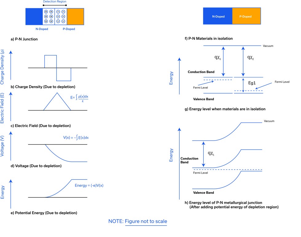
Figure 6a) Shows a P-N junction. Electrons diffuse from the N-material into the P- material and in the process leave positively charged atoms/molecules. Similarly, holes diffuse from the P-material to the N-material and in the process leave negatively charged atoms/molecules.
Figure 6b) shows the charge density.
Figure 6c) shows the Electric filed, E, where

ε is dielectric constant and ρ is charge density.
Figure 6d) shows the resulting voltage, where:
Figure 6e) shows the resulting potential energy, -eV. This is the amount by which the bands have to be bent or adjusted as will be shown next to account for diffusion.
Figure 6f) shows a P-N junction in isolation (no metallurgical contact) and Figure 6g shows the corresponding band diagram. Note that the electron affinities of N- and P-type materials are the same as they are not affected by the type of doping. Eg is the band gap. The Fermi level is close to the conduction band in N-type materials and close to the valence band in P-type material. qχ1 and qχ2 are the electronic affinities defined as the energy required to remove electrons from the bottom of the conduction band to the vacuum just outside the crystal. qχ1 is equal to qχ2 for a homojunction but is different for a heterojunction. Affinity is a very important and useful parameter in drawing band diagrams of heterojunctions.
Figure 6h) shows the energy band diagram of a P-N junction (in metallurgical contact). Note the bands have been bent by an amount shown in Figure 6e also note Fermi Level is constant throughout.
MESFET (Metal Semiconductor Field Effect Transistor)
Before we discuss pHEMT, let’s take a look at MESFET operation, which will help set the foundation for an understanding of pHEMT and its advantages.
In MESFETs, GaAs is the semiconductor material of the active layer/channel, and the gate is formed by metal-semiconductor junctions, as shown in Figure 7.
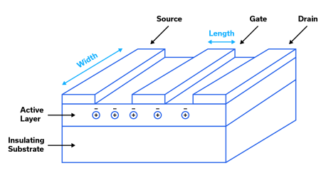
The channel is doped with n-type impurities, resulting in free electrons and ionized donor atoms. By applying a negative voltage of proper magnitude from gate to source, channel width can be pinched, and in the extreme, the channel can be closed completely, so no current flows from source to drain. This voltage is called pinch-off voltage, VP. The only drawback in MESFET is that positively charged ions slow down the electrons travelling from source to drain. In technical literature this is called coulomb scattering. HEMTs/pHEMTs are designed to eliminate coulomb scattering and speed up electron flow, thereby increasing frequency of operation.
MESFETs were extremely popular in the 80’s and 90’s for use in microwave amplifiers, switches and other components. pHEMT eventually supplanted MESFET as a preferred technology, resulting in the closure of most MESFET foundries and the conversion of many to the pHEMT process.
Heterojunction-Types [1]
As stated previously, pHEMTs/HEMTs speed up electron flow in the channel by using heterojunctions to avoiding coulomb scattering. When two different types of semiconductor materials (Material #1 and Material #2) are joined together side by side, metallurgically, three different types of energy band types can result, as shown in Figure 8. Ec and EV are conduction and valence band energy levels, and qχ is electron affinity.
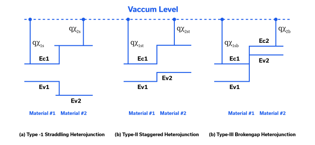
Straddling heterojunction is the type of junction used in HEMTs/pHEMTs as it enables the 2D-electron gas formation necessary for pHEMT operation as shown below.
HEMT/pHEMT
Now let us review heterojunctions used in HEMTs/pHEMTs and how they help improve electron mobility. Figure 9 shows an n-type doped AlGaAs, a p-doped GaAs heterojunction and the corresponding band diagram.
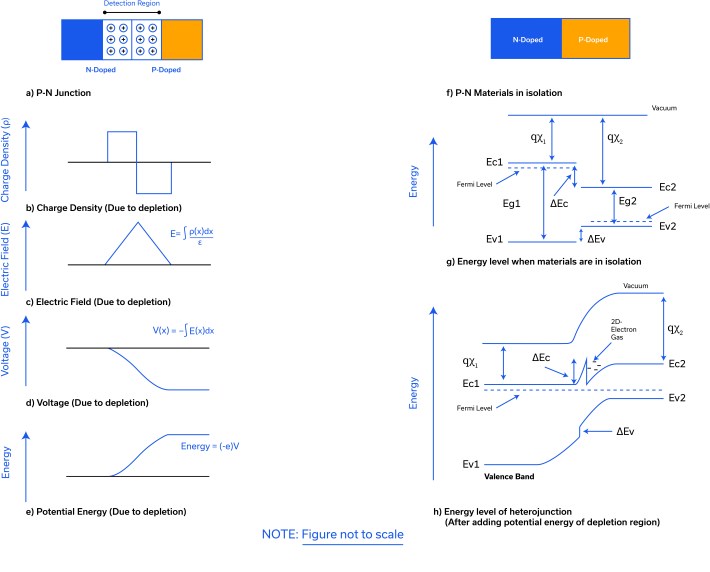
Figure 9a) to 9e) show a Hetero P-N junction, charge density, Electrical Field, Voltage and Potential energy, respectively. Note the similarity to Figures 6a to 6e illustrating Homo junction.
Figure 9f) Shows a P-N hetero junction in isolation (no depletion region).
Figure 9g) shows the energy diagram corresponding to 9f). Note that the band gaps Eg1 and Eg2 are different, Eg1 is wider than Eg2. Also note that the electron affinities qχ1 and qχ2 are different; qχ1 is less than qχ2. This results in a conduction band discontinuity of ΔEc and valance band discontinuity of ΔEv. This property is the key for pHEMT operation as we will show.
Now let us review the band diagram of the hetero junction in metallurgical contact (see Figure 9e). Up to the junction, bands bend and look similar to those in a Homo junction. At the junction, band discontinuities ΔEc and ΔEv need to be accounted for, and the result is a triangular well where electrons accumulate. This is called a 2D-electron gas. When the P-type material is lightly doped or undoped, electrons in the 2D-electron gas region encounter little or no charged atoms when in motion, there is no coulombic scattering, and they flow with higher mobility, which reduces the transit time and increases frequency of operation as we will see later.
This discovery of 2D electro gas was first reported by Bell Labs in New Jersey in 1978 [7]. Mimura of Fujitsu added a gate to this structure, converted it into a 3-terminal FET, and called it High Electron Mobility Transistor or HEMT [8,9]. Mimura reported mobility enhancement by a factor of 5.5 at 77K and 1.23 at 300K. This invention fueled further research, and several smart innovations followed such as use of different materials and doping profiles [1,4,6].
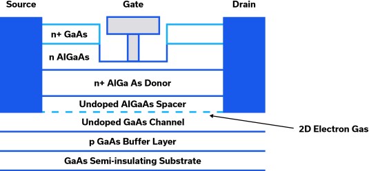
The epitaxial structure of a HEMT device is shown in Figure 10[6]. Source and drain are close to the 2D-electron gas layer, and the gate is on an n-AlGaAs layer.
The operation of HEMT structures is explained by Mimura [8] in his original review paper as follows.
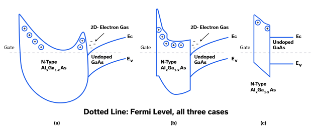
Figure 11(a) shows a thick AlxGa1-xAs layer. This results in a depletion region close to the gate, a charge neutral region in the middle and a depletion region at the hetero interface of the AlxGa1-xAs/GaAs layer. Electrons from the n-Type AlxGa1-xAs are transferred to the undoped GaAs side and stay there in the quantum well. Here the charge-neutral region shields the electric field from the gate. The charge flow in GaAs therefore cannot be controlled and is not useful.
D-mode HEMT (Figure 11(b)) features a medium thickness AlxGa1-xAs layer where the depletion regions merge, and gate voltage reaches the electron accumulation layer and controls electron flow.
E-Mode HEMT (Figure 11(c)) has a thin AlxGa1-xAs layer, where “the pinning point of the Fermi level on the AlGaAs surface is below the conduction band of the GaAs layer, the electron accumulation layer disappears when a positive gate voltage higher than the threshold is applied, and an electron accumulation layer is induced at the interface.”[9]
One early application of E-mode HEMTs was in low noise amplifiers used in radio telescopes. These new devices replaced expensive parametric amplifiers. The invention has since stimulated worldwide development of HEMTs/pHEMTs for countless applications.
In D-mode (Depletion mode) pHEMTs, the FET is “ON” with zero gate voltage, and source-to-drain resistance is low due to the presence of 2-D electron gas. If drain-to-source voltage is applied prior to the application of gate voltage, drain current will be very high, and the device may be destroyed due to overheating. To avoid this, voltage sequencing is needed as follows:
1) Apply gate voltage beyond pinch-off first
2) Then apply drain to source voltage
3) Lastly, adjust gate voltage to realize desired drain current.
This may require external voltage sequencing circuitry, which increases cost and complexity. Self-biasing is sometimes used to avoid this.
In E-mode (Enhancement mode) pHEMTs, 2-D electron gas is absent at zero gate voltage and drain-to-source resistance is high. Therefore, application of drain-to-source voltage prior to gate voltage is okay and simplifies biasing circuit design.
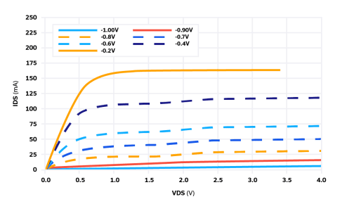
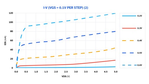
Figures 12 and 13 show I-V curves of D- and E-Mode pHEMTs.
In the D-mode pHEMT (Figure 13)[10], with VGS =-0.2V, IDS is ~170 mA and with VGS = -1V, IDS is almost 0 mA, as expected.
In the E-mode FET (Figure 13)[11]the behavior is quite the opposite, with low VGS = +0.2V, IDS is ~0mA and with VGS = +0.6V, IDS is ~100 to 120 mA, as expected.
pHEMT amplifiers generally offer low noise figure, medium power, high OIP3 and good gain, which makes them attractive for a wide range of application requirements.
Commercial Wafers: An Example [12]
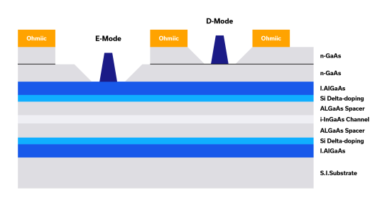
Commercial foundries now routinely offer E-D mode wafers, which enable realization of E- and D-mode FETs on the same wafer. Figure 14 shows an example. Here, the semiconductors are AlGaAs and InGaAs, each of which has a different lattice constant, hence forming a pseudomorphic junction. Silicon Delta-doped AlGaAs (high concentration of dopants in a thin layer) act as donors. Intrinsic InGaAs acts as the channel. A thin layer of AlGaAs spacer is added on either side of the i-InGaAs channel to separate the InGaAs channel from the Delta doped layer to avoid coulomb scattering.
Reliability [See Note 1]
pHEMT technology has matured since its invention and has demonstrated outstanding reliability over the course of its evolution. pHEMT devices routinely pass High Temperature Operating Life Tests (HTOL) at a junction temperature (Tj) of 150℃ over 1000 to 5000 hours. In operating conditions at max operating temperature, a well-designed amplifier has junction temperature of 130℃ or less. Therefore, pHEMT offers excellent reliability even at the highest rated operating temperature.
As an example, Mini-Circuits’ PMA3-83LN+ passed 1000 hours of HTOL at a junction temperature of 180℃ on 78 samples. Computed Mean-Time-To-Failure (MTTF) based on these tests is shown in Figure 14.
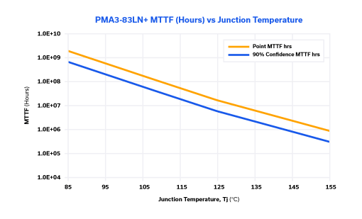
Note that at max operating temperature and nominal current, Tj is 109℃. From Figure 15, at 109℃ , MTTF is 3.8 x10⁷ hours (or 4300 years) at 90% confidence. This is extremely reliable.
Mini-Circuits parts are designed with high reliability as a design requirement. Designers take into consideration thermal aspects and target Tj to be below 130℃ at the highest ambient temperature. This is validated with thermal imaging, and reliability is validated with HTOL (note 1). If these conditions aren’t met, the product is redesigned.
Circuit Applications
A few examples of pHEMT amplifier designs include low noise and wideband models in the PMA-, PHA-, and AVA-series to 43.5 GHz and beyond. Mini-Circuits offers a wide selection fully GaAs based pHEMT amplifier portfolio as of July 2021. Several new amplifiers are currently in various stages of design and qualification.
In addition to amplifiers, Mini-Circuits also offers high-speed switches with built-in drivers. For example, the M3SWA2-63DRC+ SPDT switch achieves nanosecond switching speed to 6 GHz. This model uses a single die as opposed to two-die solutions (such as CMOS driver + pHEMT/MESFET RF die) to lower cost. It also has wider bandwidth of DC to 6 GHz vs. 0.5 to 6 GHz using a two-die solution (as in VSWA2-63DR+).
Conclusion
Heterojunction technology offers the freedom of band gap engineering to epi designers and has resulted in a mature, reliable technology used in pHEMTs. Mini-Circuits has designed and produced a wide variety of low-noise and wideband amplifiers and switches using this technology to 43.5 GHz. Besides pHEMT, Mini-Circuits also uses Heterojunction Bipolar Transistor (HBT) technology, which has certain advantages over pHEMT such as better 1/f noise[17]. HBT will be covered in the next article in this series.
Glossary of Terms
MMIC: Monolithic Microwave Integrated Circuit
FET: Field Effect Transistor
HEMT: High Electron Mobility Transistor
pHEMT: Pseudomorphic High Electron Mobility Transistor
LED: Light Emitting Diode
HBT: Heterojunction Bipolar Transistor
Primitive Cell: The smallest assembly of atoms that can be replicated to form the entire crystal
Lattice Constant: Dimension of the primitive Cell
Epitaxy/Epi: unique growth mode in which the crystalline structure of the grown film matches that of the substrate
Band Gap: Energy gap from top of valence band to bottom of conduction band in semiconductors and insulators
References
- S.M.Sze et.al., “Physics of Semiconductor Devices”, Wiley, 2021
- 14.12: Mole Fraction – Chemistry LibreTexts
- A Primer on RF Semiconductors (MMICs) – Mini-Circuits Blog (minicircuits.com)
- Fazal Ali & Aditya Gupta, “HEMTs and HBTs: Devices, Fabrication and Circuits”, Artech House, 1991.
- https://ocw.mit.edu/courses/materials-science-and-engineering/3-091sc-introduction-to-solid-state-chemistry-fall-2010/electronic-materials/14-semiconductors/MIT3_091SCF09_lec14.pdf
- Sammy Kayali, George Ponchak, Roland Shaw, “GaAs MMIC Reliability Assurance Guideline for Space Applications”, JPL Publication 96-25, December 15, 1996
- R. Dingle et.al., “Electron mobilities in modulation‐doped semiconductor heterojunction superlattices”, Appl. Phys. Lett. 33, 665 (1978)
- T. Mimura, S. Hiyamizu, T. Fujii, and K. Nanbu, “A new field-effect transistor with selectively doped GaAs/n–Al Ga As heterojunctions,” Jpn. J. Appl. Phys., vol. 19, no. 5, pp. L225–L227, 1980.
- Takashi Mimura, “The Early History of the High Electron Mobility Transistor (HEMT)”, IEEE Trans on MTT, PP 780-782, Vol 50, No.3, March 2002
- https://www.minicircuits.com/pages/s-params/SAV-331+_GRAPHS.pdf
- https://www.minicircuits.com/pages/s-params/SAV-581+_GRAPHS.pdf
- Y. Y. Hsieh et.al, “Enhancement and Depletion-Mode pHEMT Using 6 inch GaAs Cost-effective Production Process”, Page 111-114, 2004 IEEE CSIC Digest
- T. Mimura, “Semiconductor device,” Japanese Patent 1 409 643, Nov. 24, 1987.
- U.S.Patent 4,424,525
- https://www.sciencedirect.com/topics/materials-science/heteroepitaxy
- https://blog.minicircuits.com/additive-phase-noise-in-amplifiers/
- https://youtube.com/watch?v=5FjSxfp8ueI&feature=share (Excellent tutorial on Hetero Junctions)
Notes
[1] The above mean time to failure (MTTF) and or Failure in Time (FIT) figures are provided only as a potential guideline and merely reflect Mini-Circuits’ opinion or recommendation. Using MTTF/FIT calculations alone are not appropriate to predict the life expectancy of a model; other factors such as heat dissipation, specific operating current and voltages, duration of use, actual stress and signal levels, as well as other environmental conditions are just a few factors that also need to be considered. Accordingly, the MTTF/FIT figures provided do not constitute or create a warranty, express or implied, concerning future performance or the life expectancy of the model or otherwise.


