Extending the Performance and Frequency Envelope for QFN Packaging Technology
Erick Olsen, Radha Setty and Chris Simmonds
High-performance, millimeter-wave (mmW) Monolithic Microwave Integrated Circuit (MMIC) products and cost-effective surface mount lead-frame-based packaging typically don’t come up in the same conversation, and for good reason. Just two to three years ago, it was difficult to conceive of operating at frequencies above 20 GHz without considering an expensive, open cavity, High Temperature Co-fired Ceramic (HTCC) package or resorting to more bespoke chip and wire assemblies.
Why the need for these expensive solutions? The answer is simple. At mmW frequencies, every dB of signal strength is hard won. Traditional low frequency materials, like FR-4 for printed circuit boards or epoxy for molded packages, have excessive losses at mmW frequencies. For example, even newer materials like Hemeixin’s Megtron 6 that operate well up to 20 GHz have a dissipation factor (Df) of 0.04 at 12 GHz, compared to TLY-5Z from Taconic, which has a Df 0.0015 at 10 GHz. Although these materials are cost effective, their lower performance above 20 GHz combined with the potential need for extra gain stages, accompanying support circuitry and more complex signal processing are an ineffective trade-off for the lower cost materials. Thus, more exotic and more expensive materials are needed to mitigate parasitic losses.
Air cavity packaging also reduces losses. However, these types of assemblies often require manual manufacturing methods. The resulting cost of materials and manufacturing methods make up a significant portion of the solution bill of materials (BOM) cost, and therefore a natural target for optimization. Meanwhile the growing attractiveness and demand for high volumes in the mmW bands is adding further cost pressure.
In response, Mini-Circuits has developed innovative packaging techniques to push the frequency range of over-molded packaging (e.g. the compact “quad flat no-lead” or QFN chip) up to 50 GHz. These techniques have been used successfully to design passive components including fixed attenuators, equalizers, splitters and reflectionless filters, as well as for high-frequency active mixers, multipliers and amplifiers. This article will explore the methods used to achieve high-frequency over-molded packing solutions for active and passive components, including high frequency package synthesis through a multiphysics [1] simulation approach and manufacturing techniques.
Historical Background
For as long as RF, microwave and millimeter wave systems have been developed and deployed, circuit designers have been faced with developing high-performance circuits that can withstand the rigors of their intended applications. Early discrete implementations evolved into increasingly more integrated solutions to reduce size and cost, as well as improving part to part uniformity. The methods of maintaining optimal operating conditions and protecting the circuitry against environmental hazards evolved in lock step. Electrical and mechanical requirements have never been mutually exclusive, though the engineering approaches to meeting their interrelated specifications have often been accomplished piecewise due to the limitations in analysis software, and sufficiently accurate simulation models. As operating frequencies increased, so too, did the difficulty of meeting these combined requirements.
Operating at mmW bands is hardly a new concept. J.C. Bose presented his research on mmW to the Royal Institution in London in 1897 [2][3][4], where he showed operation and measurements as high as 60 GHz (Figures 1. and 2.). Similar, independent work was demonstrated by Lebedew in Moscow, also up to 60 GHz [5].
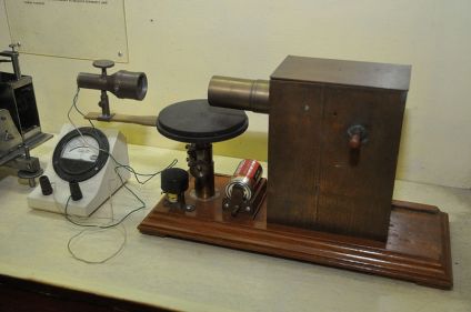
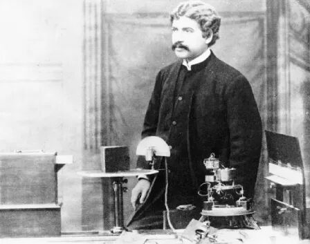
Figure 2: Sir J. C. Bose demonstrating his wireless millimeter wave (microwave) experiments at the Royal Institution, London in January, 1897 [2]
mmW applications and frequency allocations have existed for some time for uses including navigation, radiolocation, Industrial, Scientific and Medical research, space exploration, point-to-point communications and commercial telecommunications backhaul. In the early days of these applications, packaging the systems and supporting components was typically focused on physical protection, as they were often contained within fixed, environmentally-controlled enclosures. Protecting the individual active components was of less concern. That is not to say the packaging was not important. Often, these systems were built into metal housings, and dealing with thermal management, mode suppression, and shielding was accomplished effectively, but done empirically, and with minimal regard to cost. It was all about getting the system to work. The volumes were low, so cost was less of an issue.
Research and low-level production of broadband and mmW systems were more tolerant of this hands-on approach, and the balance of supply and demand was adequately met. Fast forward to the era of commercialized telecommunications, and the situation is far different. mmW bands, once the domain of research and niche applications, have become mainstream. 5G and massive MIMO[1] promise to accelerate the demand for mmW systems, with as much as 45% of the predicted 24GB of individual monthly data consumption to be delivered by 5G networks [6]. As such, in November 2019, the World Radio Communication Conference (WRC-19), concluded that 5G should be allocated, on a global basis access to certain sections of these mmW bands [7]. Applications that are part of the IoT ecosystem will also drive high-volume utilization of mmW frequencies.
The benefits of broadband and mmW will be a boon to a number of industries. Commercialization and strong demand, however, in no way lessen the performance requirements or the challenges of meeting them. To the contrary, the former depends entirely on the latter. The challenges of atmospheric attenuation, scattering (e.g. urban canyons), and poor penetration all necessitate high-density point-to-point deployments to reduce the impacts noted. At the core of these systems are high-performance nanometer silicon, GaAs and GaN electronics that need to deliver leading edge capabilities at a cost-effective price point, “cost-effective” being the operative word. The increased demand for high-performance, broadband mmW systems will not be serviceable/scalable if the supporting solutions can not meet the cost structure needed.
Searching for a Solution to the Cost-Performance Dichotomy
Two years ago, Mini-Circuits foresaw the demand curve and the simultaneous need for high-performance and cost-competitive mmW solutions, and launched an internal research and development effort to solve the challenge. The two-year effort was a substantial investment in time, resources and opportunity cost, and one could argue that there are less expensive paths to follow. Historically, it was normal practice for mmW component vendors to deliver their solutions only in die form, eliminating the package entirely. While some legacy applications can afford this manually intensive approach, most customers working in these higher frequency ranges have neither the capability nor the desire to deal with bare die and chip and wire assemblies. With shorter time to market, smaller engineering teams, and greater cost pressures, customers have realized that the performance benefits don’t outweigh the higher total cost of ownership of bare die solutions.
Another often-used approach is the aforementioned open cavity package form factor. HTCC solutions have been around for decades and are widely accepted in the industry. However, the more expensive assembly process results in higher component costs which again make it difficult, if not impossible to meet the cost targets for today’s high volume mmW applications.
Die on carrier (ceramic, alumina or other high-end substrate) is a hybrid method between bare die and air cavity packaging, but this method offers little physical protection for the active components. These carriers often need to be assembled into expensive hermetic enclosures or protected via conformal coating which carries a higher initial and/or rework cost (e.g. applying, removing and reapplying conformal coating).
After evaluating many of these options, Mini-Circuits decided to look internally and leverage in-house capabilities to deliver the high-performance packaging we needed. Working with our integrated circuit (IC) designers and package development team in Malaysia, Mini-Circuits researched new ways to apply our packaging capability to the problem of mmW performance. Initial analysis identified three areas beyond the circuit design itself that could contribute meaningful improvements to extending the frequency range of QFN packaged components. These include simulation enhancements, package components and manufacturing techniques.
Simulation Enhancements
Traditionally, MMIC products are designed with most of the focus on the electrical simulation at the IC level, with simple models to represent the package interconnects and grounding of traditional plastic, over-molded packaging. At frequencies below 10 GHz, this approach arrives in the ballpark of actual performance with minimal simulation spins to account for the package. Above 10 GHz, the electrical-only simulation approach becomes inaccurate, and around 50 GHz, this approach won’t even yield a close approximation to real world behavior.
To accurately predict IC operation at mmW frequencies, 2.5D or 3D electromagnetic (EM) simulations are essential. These tool suites are now widely available and can greatly increase modelling accuracy. They do, however, trade modelling accuracy for longer development time, so they must be applied judiciously.
The process of IC simulations followed by EM simulations of the complete packaged solution, if applied by brute force, is slow and inefficient. At Mini-Circuits, we’ve looked at the entire design process, and optimized the application of these tools to the tasks where they are best suited. Our unique multiphysics simulation approach speeds the entire design process while ensuring close agreement between modelled predictions and measured results.
Package Components
Even with luxury of an in-house IC packaging line, it can be easy to take the status quo as given. But the status quo was not going to deliver the needed mmW performance. Analyzing the packaging materials uncovered some basic assumptions that were limiting performance at high frequencies. Combining this detailed material analysis with targeted 3D EM simulations yielded new options to optimize performance in the mmW range.
Manufacturing Techniques
As with the packaging components, assembly techniques have a considerable effect on overall product performance. Specifically, the wirebond interconnects, their method of attachment and physical layout have the greatest impact on the frequency response of the package. Detailed analysis of these features of the MMIC assembly led to innovative bonding techniques that have shown IC performance beyond the intrinsic performance of the die itself.
Innovating the QFN Production Workflow
The results of the aforementioned research provided valuable insights into the limitations imposed by the standard QFN production flow, and more importantly, uncovered multiple options to address these limitations. We used these insights to approach the task of over-molded mmW component packaging in a holistic way, focusing on three primary, interrelated factors:
- Die improvements
- Leadframe optimization
- Non-RF interconnects
Each of these factors will be discussed in turn below with examples of recent QFN components exhibiting excellent performance up to 50 GHz.
Die Improvements
The contribution of the IC circuit design to the overall solution performance cannot be understated, but the interface between the IC and the package is critical. Bondpad geometry and transition were both important factors in optimizing performance. There is always a tradeoff between the number of RF bondwires and the accompanying bond pad size. Simply adding more bondwires doesn’t reduce the series inductance as mutual inductance diminishes the benefit of additional wires. Also, a larger bondpad to accommodate the extra wires adds unwanted capacitance. Our solution was to develop bonding techniques that reduced effective bondwire inductance and simultaneously reduced parasitic capacitance to ground, resulting in an interconnect structure that better approximates a 50Ω transmission line. The better match of the bondwire structure provided flexibility to tune the transition on the die, again optimizing the frequency response.
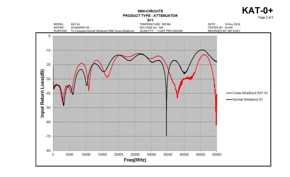
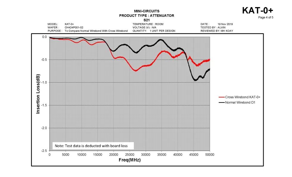
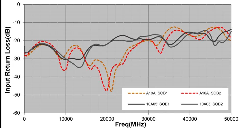
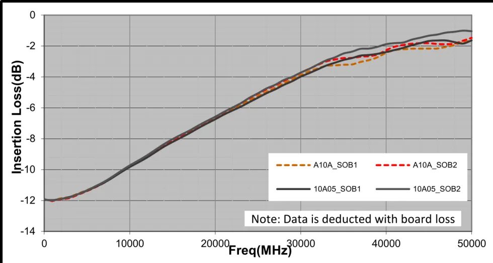
The KAT-series of precision attenuators is one example of Mini-Circuits’ patent pending bonding technique. Based on the YAT-series of 26 GHz attenuators, we were able to extend the desired frequency response to 43.5 GHz (released in late 2019 as KAT-x+). With further refinements, a new family of attenuators will be released in 2020 that will operate up to 50 GHz (Figure 3.) where both the insertion loss and return loss were measurably improved up to the 50 GHz band edge.
This same approach was used in a soon-to-be-released family of DC to 50 GHz slope equalizers EQY-x-503 (Figure 4.). In these new equalizer products, the optimized bonding delivered more consistent return loss across the band, as well as improved monotonicity of the response.
Lead Frame Optimization
The package anchor point for the bondwire connection is equally important to the bond pad design on the die itself. This is where in-house packaging capability was of great benefit. We optimized the size and location of the leadframe RF bondpads (relative to the other package connections) based on 3D simulations, and we quickly created prototypes to validate the simulations, shortening the learning cycle.
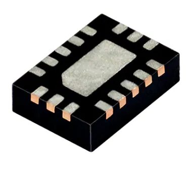
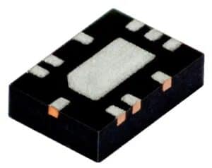
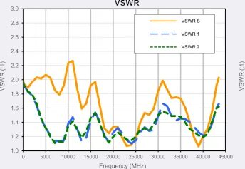
Another improvement was in the overall design of the leadframe itself. Specifically, the EM simulations showed unwanted coupling between pins, even if unconnected internally or grounded externally. This coupling substantially degraded high frequency response. The EP2KA+ two-way MMIC splitter (10 to 43.5 GHz) is a perfect example of this pin optimization approach. We started with the same package as the MGVA-82+ (DC to 5.2 GHz dual matched amplifier), and by selectively removing pins from the leadframe (Figure 5.), were able to measurably improve the input to output isolation, as well as the amplitude and phase unbalance. The leadframe bond pad optimization also improved input/output VSWR to better than 2:1 over the majority of the band (Figure 6.).
Non-RF Interconnects
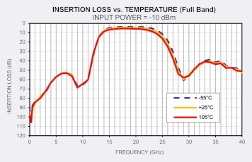
At mmW frequencies, confining the RF signal, and reducing unwanted coupling is a challenge, as described above. While the RF connections are often the focus of the design, the non-RF connections, if overlooked, also contribute to performance degradation at higher frequencies. There are times when these package contacts can’t be eliminated, so Mini-Circuits developed a patent-pending technique which takes advantage of these extra connections to isolate portions of the IC, improving the input to output frequency response. Our line of reflectionless high pass filters used this approach to achieve insertion loss as low as 0.7 dB up to 30 GHz, while maintaining excellent low frequency stop band performance (Figure 7).
Conclusion
In this paper, we have presented multiple innovative approaches to extending the useful operating frequency range of traditionally low cost, overmolded plastic packaging technologies. Resulting from over two years of research, and through co-development, multiphysics co-simulation, and refining established methods and techniques, we have developed and produced multiple products for use in mmW applications, including: attenuators, equalizers, splitters and reflectionless filters. These innovations have enabled us to meet mmW performance requirements demanded by the telecommunications, aerospace, defense, and test and measurement markets, using cost-effective, industry-standard QFN packaging technology.
References
- [1] https://commons.wikimedia.org/wiki/File%3AMicrowave_Apparatus_-_Jagadish_Chandra_Bose_Museum_-_Bose_Institute_-_Kolkata_2011-07-26_4051.JPG
- [2] Bose Institute, Founder J.C. Bose: http://www.jcbose.ac.in/founder
- [3] J.C. Bose, “On the determination of the wavelength of electric radiation by a diffraction grating”, Proc. Roy. Soc., vol. 60, pp.167-178, 1897.
- [4] J.C. Bose, Collected Physical Papers. New York, N.Y.: Longmans, Green and Co., 1927
- [5] P. Lebedew, “Ueber die Dopplbrechung der Strahlen electrischer Kraft,” Annalen der Physik und Chemie, Series 3, vol. 56, no. 9, pp. 1-17, 1985
- [6] Mobile traffic outlook, Ericsson, November 2019, https://www.ericsson.com/en/mobility-report/reports/november-2019/mobile-data-traffic-outlook
- [7] ITU World Radiocommunication Conference agrees key parameters for future communication technologies, Sharm El-Sheikh, 22 November 2019, https://www.itu.int/en/mediacentre/Pages/2019-PR24.aspx


