Linearity – Cascaded P1dB and IP3 for a Simple Microwave Front-End
When examining a device data sheet, linearity parameters P1dB and IP3 are straightforward and relatively easy to apply during the design process. Once several components are connected in series in a design, complex equations governing cascaded P1dB and IP3 must be utilized to determine the overall linearity performance of the system or subsystem. The equations utilized to compute P1dB and IP3 provide a means of achieving accurate results in the absence of expensive simulation software. Even though the effect of VSWR interactions between stages is not included when performing the calculations, the results are a good first order approximation of the cascaded performance of the system. The purpose of this application note is to review P1dB and IP3 in general, and to compute these parameters for a basic, three-component RF front end. Other application notes in this series will delve further into the cascading of P1dB and IP3 as the system includes additional nonlinear components such as those utilized in frequency conversion and the accompanying IF components.
Thinking Linearly – P1dB and IP3
P1dB and IP3 (and, to a lesser extent, IP2) are the gold-standard parameters for system linearity, whether the system is a receiver, transmitter or transceiver. Receiver designers tend to look at input P1dB and IP3, transmitter designers work mostly with output P1dB and IP3, and transceiver designers, well, both. For the purpose of this application note, we will first focus on computing output P1dB (OP1dB) and output IP3 (OIP3), then show how one can back into IP1dB and IIP3. Transitioning seamlessly between the input and output linearity parameters through the gain of the system will become apparent. Figure 1 shows that a linear gain response curve (with a theoretical, dashed line extrapolation) and a third order (cubic) intermodulation distortion (IMD) response (again, with a theoretical extrapolation) will intersect at a purely theoretical third order intercept point (TOI, or, more commonly IP3). OIP3 is determined graphically by the projection of IP3 onto the Y-axis (Pout) and IIP3 by the projection of IP3 onto the X-axis (Pin). The solid curves, which are representative of the physical operating characteristics of the amplifier or system, tend to exhibit compression as they approach the system’s operating output power limit, and saturation once that limit is reached. Figure 1 also shows the point at which the gain has compressed by 1 dB, which is projected as OP1dB on the Y-axis (Pout) and IP1dB on the X-axis (Pin).
![Linearity – Cascaded P1dB and IP3 for a Simple Microwave Front-End 1 Figure 1: POUT vs. PIN curve showing IP1dB, OP1dB, IIP3 and OIP3. [1]](https://www.mcdi-ltd.com/wp-content/uploads/2022/10/Cascading-P1dB-IP3.webp)
Since both input and output P1dB and IP3 are reflected about the gain (“linear response”) curve, we can expect them to be directly related by the system gain, as we will see in a subsequent section.
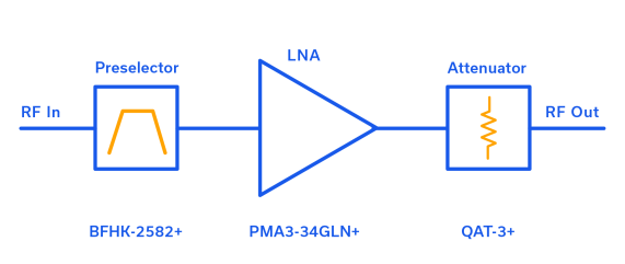
The system we utilize as an example, shown in Figure 2, is an RF front end capable of covering the 24000 – 27500 MHz frequency band. The design includes all SMT-style components that enable the RF front end to be constructed on a very small footprint. The device packages measure 4.5 x 3.2mm for the BFHK-2582+ bandpass filter, 3 x 3mm for the PMA3-34GLN+ LNA, and 2 x 2mm for the QAT-3+ attenuator. Combined, these SMT components only occupy a total area of 27.4 square mm. A possible application of this structure would be a point-to-point microwave system covering the 24250 – 26500 MHz frequency band. Although the components shown in Figure 2 are not typical of the style of components utilized in such an application, inserting novel parts into a legacy application always proves more interesting than discussing the application notionally, or making use of older technology parts.
The salient features of the three components are shown above the block diagram of Figure 2, and the part numbers are listed beneath the blocks as links to their respective device dashboards.
- Preselector (BFHK-2582+): 24000 – 27500 MHz (2.23 dB insertion loss)
- LNA (PMA3-34GLN+): 20.41 dB gain at 26500 MHz
- Attenuator (QAT-3+): 3.15 dB at 26000 MHz
OP1dB and OIP3 Levels in the System
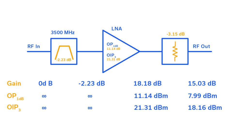
As our attention turns to OP1dB and OIP3 for passive components such as the preselector and 3 dB attenuator, it becomes obvious that these components are totally linear, and that they don’t have gain (or loss) compression, nor do they introduce intermodulation distortion. Consequently, as shown in Figure 3, the cascaded levels for OP1dB and OIP3 after the preselector both remain at infinity. Granted, all passive components do have thermal limitations, but filter loss and attenuator loss simply don’t behave nonlinearly.
For the PMA3-34GLN+ LNA, OP1dB and OIP3 are taken from the data sheet at 26500 MHz, the same frequency at which the gain was also determined. Following the LNA stage, which is most certainly nonlinear, cascaded OP1dB and OIP3 values begin to take shape. In fact, both the OP1dB and the OIP3 cascaded performance levels are exactly those of the PMA3-34GLN+ device itself, unaffected by the linear bandpass filter/preselector which precedes it. A careful examination of the cascaded OP1dB and OIP3 values downstream from the QAT-3+ attenuator shows that each of their values has merely been reduced by the loss of the attenuator (3.15 dB). So why is the calculation of cascaded OP1dB and OIP3 purported to be so arduous when it seems so intuitive, and can even be done by inspection at times? Well, as the old adage goes, the devil is in the details. Be aware that the equations governing the cascading of OP1dB and OIP3 parameters are somewhat complex, and that multiple nonlinear stages complicates matters significantly. In this case, we have just a single nonlinear component: the LNA.
Converting OP1dB and OIP3 into their IP1dB and IIP3 Counterparts
Input P1dB and input IP3 can be determined directly from OP1dB and OIP3 for the entire cascade by passing each of them through the gain of the system, with one important difference. By definition, OP1dB is the output power level at which the linear gain has compressed (experienced a reduction of) 1 dB. Consequently, the equation relating IP1dB to OP1dB must account for this 1 dB of gain compression as follows:
IP1dB = OP1dB – (Gain – 1), or: IP1dB = 7.99 dBm – (15.03 dB – 1 dB) = -6.04 dBm. The term in parenthesis is referred to as G1dB, or the 1 dB-compressed value of the gain.
To determine IIP3 from OIP3 is more straightforward. The gain is simply subtracted from OIP3 as:
IIP3 = OIP3 – Gain, or: IIP3 = 18.16 dBm – 15.03 dB = 3.13 dBm As a practical matter, referencing P1dB to the input means that, if the signal is “gained up” as with our system, gain compression that occurs at the output must be referenced back to the lower, input level at which it occurs, taking into account that the gain has compressed by 1 dB at P1dB. Likewise, IP3, which is determined by extrapolating the linear gain and third order IMD curves, must be referenced back to the lower, input level as well, but in this case by subtracting out the linear gain.
Going Nonlinear – Next Steps in Cascading P1dB and IP3
An RF front end was presented for the 24250 – 26500 MHz frequency band comprised of all SMT parts. Block diagrams were presented for the basic RF front end followed by a more detailed figure showing the calculated, cascaded parameters. Conversion between OP1dB and IP1dB, and OIP3 and IIP3 was shown as well as a practical explanation given. A follow-up application note to this provides the designer a deeper understanding of the equations behind the cascading of P1dB and IP3 as the system expands to include additional nonlinear components (amplifiers/mixers) such as those utilized in the RF, frequency conversion and IF domains.
References
- What is IP3? Everything RF, December 8, 2017, Anjali Iahoti


