MMIC Amplifiers with Shutdown and Bypass Features De-Mystified
Overview
Mini-Circuits’ TSS- and TSY-families of MMIC amplifiers feature a versatile combination of performance characteristics including high dynamic range and very low noise figure with wideband frequency coverage from VHF up to mmWave applications. These product families also include additional features of shutdown and bypass functionality. These features often lead to customer questions about the difference between bypass and shutdown, which products have which features, and the benefits of each. This article will explain how these features work, and provide an overview of some of the applications are where shutdown and bypass functions are most commonly used.
Amplifier Shutdown Functionality and Applications
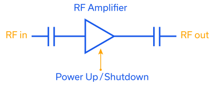
Just like it sounds, shutdown functionality provides the RF system designer the ability to power down an RF amplifier in certain conditions. A block diagram for an RF amplifier with shutdown functionality is shown in Figure 1. This amplifier includes an added control signal for power up and shutdown states. This is an external DC control signal to the RF amplifier that controls whether the RF amplifier is powered up or powered down. In the powered-up mode, the RF amplifier bias current is fully on, and the RF amplifier performs to the specifications defined in the data sheet. In shutdown mode, the bias current of the RF amplifier is collapsed to a small fraction of the normal bias current near 0 amps.
It’s worth noting that in the shutdown mode, it is expected that the amplifier will not be used in an active signal chain. With no current in the amplifier, the amplifier has no gain and no bandwidth, anda signal path that contains the amplifier in shutdown mode can no longer pass signals from the input to the output. In shutdown mode, the 50W match that the amplifier maintains when active (on) may no longer be maintained. The input and output ports of the amplifier therefore become high-impedance, and this may introduce instabilities in the signal path. Thus, it is required that the 50W match be somehow maintained when the amplifier is in shutdown mode.
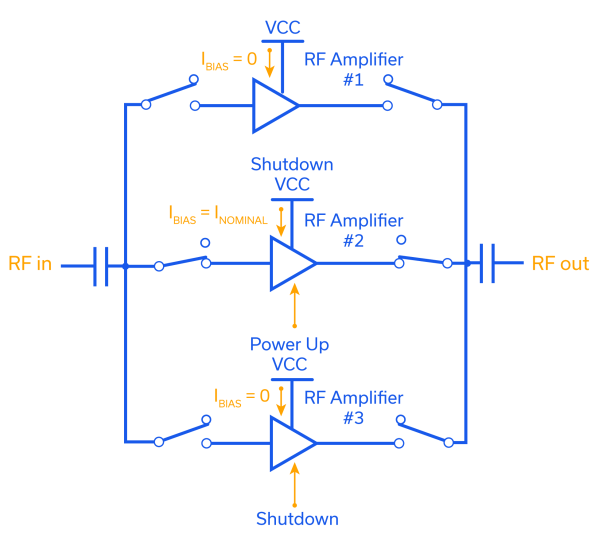
As one example of an application of the shutdown feature, a single pole, multi-throw switch may connect the RF signal chain into different RF gain blocks as shown in Figure 2. Only a single gain block will be selected out of the three amplifiers shown at any given time. It is desirable for all unused amplifiers in the amplifier bank be shut off to save DC power dissipation in the system. A typical discrete RF amplifier has no way to reduce the DC power dissipation without shutting down the power supply, which would cause problems for the active circuitry in the RF signal chain still relying on the same power supply.
It would therefore be preferable to provide an RF amplifier with the additional capability to shut the DC power dissipation off. The DC power dissipation of the amplifier bank is significantly reduced for the overall system if this shutdown functionality is available in each RF amplifier. In Figure 2, the top and bottom amplifiers have the shutdown control signal applied, so the bias current of the amplifier, IBIAS, is equal to 0 amps. The middle amplifier has the power-up control signal applied, which causes IBIAS, to be equal to the nominal current value INOMINAL.
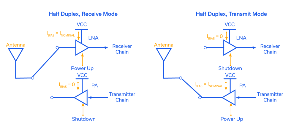
Another application where shutdown functionality is useful to save power is in the half duplex or time division duplexing (TDD) mode of operation for an RF transceiver. For TDD operation, either the transmitter or the receiver is on at any given time, but neither are ever on simultaneously. For this type of transceiver, the receive amplifier signal chain can be shut off while the transmitter is active, and vice-versa. This will reduce the total power dissipation by the duty cycle of operation for receive and transmit.
A block diagram of this transceiver functionality for half duplex operation is shown in Figure 3. For the half duplex receive mode, the power up control signal is applied to the low noise amplifier (LNA) and the receiver signal chain, and the shutdown control signal is applied to the power amplifier (PA) and the transmit signal chain. In receive mode, for half duplex operation, only the receive signal chain dissipates DC Power. The transmit signal chain is off. Likewise, in transmit mode for half duplex operation, only the transmit signal chain dissipates DC power. The receive signal chain is off.
By using the power up and shutdown control signals, only the signal path needed is powered on, and the unused signal path DC power dissipation is reduced to zero. This way, the DC power of the transceiver can be reduced through the duty cycle of the half duplex operation. If, for example, the receive and transmit mode is 50% duty cycle, the total power dissipation can be reduced by 50%.
Amplifier Bypass Functionality and Applications
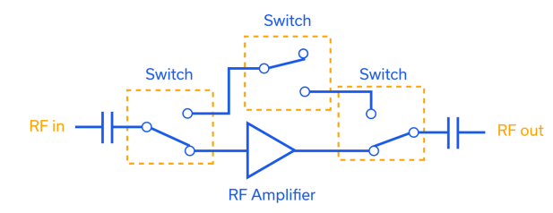
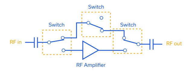
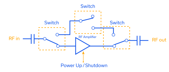
Bypass functionality provides the RF system designer the ability to remove signal gain in the RF signal chain regardless of whether the amplifier is used in an active signal path. This capability is accomplished by integrating a set of switches into the amplifier circuitry. The RF designer uses a DC control signal to route signal through the RF amplifier in “thru-mode” or “bypass” the RF amplifier in “bypass mode.” A simplified block diagram of an RF amplifier with bypass functionality is shown in Figure 4. The composite circuit consists of an RF amplifier and 3 switches. The 3 switches are single pole, double throw (SPDT) switches, and the position of the switch is determined by a control signal to the switch.. In Figure 4, the switches are set to include the RF gain block in the signal path. In Figure 5, the switches are set to bypass it.
Bypass functionality in an RF amplifier can be useful in the design of many RF signal chains. Typical RF signal chains support different gain configurations depending on the requirement for the RF signal power being either received or transmitted. Depending on the noise figure (NF) of the receiver and the power level of the received signal, it may be desirable to reduce the signal chain gain by bypassing multiple gain blocks in the RF receiver to avoid compression.
An example of this situation is shown in Figure 6. The input signal dynamic range is 40 dB, witha minimum signal level of -50 dBm, and a maximum signal level of -10 dBm. Two RF amplifiers are used with input P1dB = -1 dBm and gain = 20 dB. For an input signal level of -50 dBm, the RF amplifier is switched on, and the output signal power = -50 dBm + 20 dB = – 30 dBm. This is below the input P1dB of the next RF amplifier in the signal chain, and the RF signal chain remains in the linear region. For an input power level of -10 dBm, by comparison, the first amplifier is not compressed, and the output power is -10 dBm + 20 dB = 10 dBm which is greater than the compression point of the next amplifier. In order to avoid this, the first RF amplifier is bypassed, allowing the input power to the second RF amplifier to be -10 dBm, below the 1 dB compression point of the second RF amplifier, and the RF signal chain remains uncompressed. Bypassing in the signal chain can effectively extend the input signal dynamic range without compromising of the signal chain compression point.
Bypassing can also be used to accommodate high power levels without damaging the RF amplifiers in the signal path. In Figure 6, if both RF amplifiers are bypassed, the input signal power can be increased by > 30 dBm over the case where both amplifiers are in thru-mode, as the input P1dB is now the compression point of the bypass switch, and not the RF amplifier.

The ability to bypass gain blocks in the RF signal chain thus gives the RF system designer an additional tool to accommodate different fixed gain settings for different signal scenarios.
In a discrete COTS RF transceiver, the configuration in Figures 4 and 5 is typically achieved using 3 discrete SPDT switch components and an RF amplifier component, taking up significant board space. Integrating the switching onto the same chip as the amplifier helps reduce size and free up real estate. Additionally, the needs for bypass and shutdown functions aren’t mutually exclusive. In a discrete design, the bypassed RF amplifier still dissipates the same amount of DC power in bypass mode as it does in thru mode unless it also incorporates the shutdown functionality previously described. It is therefore desirable to have a single component solution that integrates bypass functionality and the additional capability to shut the RF amplifier DC power dissipation off in bypass mode.
Mini-Circuits’ MMIC amplifiers incorporating the bypass feature include the advantages of both shutdown and bypass functionality combined into a single component (Figure 7). In bypass mode, the SPDT switches are configured to bypass the RF amplifier, and the RF amplifier bias is off. In this configuration, the DC power dissipation of the RF amplifier is close to 0 watts, so the overall power dissipation is a small fraction of the when the RF amplifier is powered up.
Mini-Circuits MMIC Amplifiers with Shutdown and Bypass Features
Mini-Circuits’ TSS- and TSY-families of MMIC amplifiers include models with both shutdown and bypass features. Table 1 below lists these amplifier products and their associated performance characteristics. The rightmost column indicates whether the product has the shutdown or bypass feature.
| Model Number | Frequency Range (MHz) | Gain (dB) | NF (dB) | P1dB (dBm) | OIP3 (dBm) | Input VSWR | Output VSWR | Voltage (V) | Current (mA) | Feature |
|---|---|---|---|---|---|---|---|---|---|---|
| TSS-44+ | 22000-43500 | 17.6 | 3.2 | 6.9 | 12.7 | 1.37 | 1.28 | 4 | 22 | Shutdown |
| TSS-183A+ | 5000-18000 | 14.2 | 4.4 | 17.9 | 28.9 | 1.37 | 1.28 | 5 | 145 | Shutdown |
| TSS-53LNB+ | 500-5000 | 21.7 | 1.4 | 20.6 | 33.9 | 1.46 | 1.33 | 5 | 82 | Bypass |
| TSS-53LNB3+ | 500-5000 | 18.4 | 1.5 | 14.9 | 25 | 1.63 | 1.26 | 3 | 42 | Bypass |
| TSS-23HLN+ | 30-2000 | 21.8 | 1.4 | 28.5 | 42.6 | 1.92 | 1.67 | 8 | 236 | Shutdown |
| TSS-23LN+ | 30-2000 | 21.5 | 1.2 | 24.1 | 36.4 | 1.92 | 1.67 | 3 | 139/74 | Shutdown |
| TSY-172LNB+ | 30-1700 | 13.1 | 1.4 | 17.5 | 24.7 | 1.9 | 1.5 | 2.7 | 7.7 | Bypass |
| TSS-13HLN+ | 1-1000 | 23 | 1.4 | 28.4 | 42.9 | 1.43 | 1.37 | 8 | 234 | Shutdown |
| TSS-13LN+ | 1-1000 | 22.8 | 1.1 | 24.5 | 39.2 | 1.28 | 1.32 | 3 | 142/72 | Shutdown |
| TSY-13LNB+ | 30-1000 | 14.7 | 1.2 | 17.1 | 26.4 | 1.5 | 1.3 | 2.7 | 7.7 | Bypass |
Table 1: Mini-Circuits’ TSS- and TSY-families of MMIC amplifiers with shutdown and bypass features.
A Note on Datasheets for Amplifiers with Shutdown and Bypass
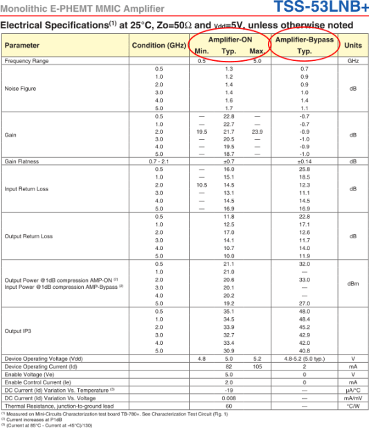
The bypass and shutdown features for the RF amplifier require that two sets of performance specifications for the product be defined. On datasheets for these products, one set of specifications is provided for the RF amplifier in the normal mode of operation when the RF amplifier is powered on and another set of specifications is given for the amplifier in shutdown mode. For models with the bypass feature, there is a separate set of specifications for when the bypass switches are off, and the RF amplifier is powered on, and a second set of specifications for when the bypass switches are on, and the RF amplifier is shutdown.
These two sets of specifications for TSS-53LNB+ are shown in Figure 8. In bypass mode, the gain of the RF amplifier is the insertion loss of the three cascaded switches as shown in Figure 4. From Figure 3, the gain of the amplifier is reduced by 20 dB to -1 dB. Additionally, in bypass mode, the OIP3 increases by > 10 dBm and the 1 dB compression point is much higher than it is in thru-mode.
Conclusion
Mini-Circuits has developed a unique family of MMIC amplifiers that opens up many applications with the addition of shutdown and bypass features. Hopefully you now have a better understanding of shutdown and bypass functionality, the differences between these features, and the applications that can take advantage of each at the system design level. If you have questions about the amplifiers presented in this article or specific requirements for your application, please contact our applications team.


