Selecting VCOs for Clock Timing Circuits – A System Perspective
Clock Timing, Phase Noise and Bit Error Rate (BER)
Timing is critical in digital systems, especially in electronic systems that feature high-speed data converters and high-resolution sampling. A clock source is the “timekeeper” and the system performance depends upon the effectiveness of this component. For some system designers, implementing a clock source automatically means using a crystal oscillator, typically a single-frequency source. But other designers, especially those tasked with synchronizing systems at multiple clock frequencies, have learned to appreciate the flexibility of using voltage-controlled oscillators (VCOs) as clock sources.
VCOs can serve as clock circuits for wireless communications networks, video broadcast systems, test equipment, and any system that requires timing synchronization for data processing, digital signal processing, or channeling logic signals. VCOs support data conversion circuits in analog-to-digital converters (ADCs) and digital-to-analog converters (DACs) and logic circuits that depend on reliable clock signals. These tunable, high-frequency oscillators are manufactured by various suppliers in many different form factors, from die to packaged devices, which makes specifying a VCO for a clock timing application, or even a traditional analog heterodyne receiver, no simple task.
Selecting VCOs for clock timing applications requires a thorough understanding of VCO specifications and an intuitive sense of how those performance parameters affect system functionality. For instance, it is critical that designers understand how phase noise in the frequency domain translates into clock jitter in the time domain. Once clock jitter (often called phase jitter) has been calculated, the designer must consider its effect on the system BER to determine if the VCO’s performance is sufficient to meet the system requirements. In this application note, we first discuss VCOs and some of their salient features. Since phase noise is such a key parameter in VCO selection, we show how spot noise measurements can be utilized to determine integrated phase noise. Knowledge of the VCO’s integrated phase noise enables us to calculate time domain phase jitter, an important step toward the end goal of determining if the chosen VCO will enable the system to meet its BER requirements.
Phase Jitter
Designing clock timing circuits involves precisely managing timing accuracy in the clock source, since any errors in clock timing can result in degraded digital system performance and data loss or corruption of data. High-speed clock signals are generally characterized by fast rise and fall times on their leading and falling edges. The steeper the slope, and the more periodic the waveform, the less noise and less timing error is introduced by the clock signal, and the less degradation to system performance.
An ideal rectangular clock waveform is shown in Figure 1a, whereas Figure 1b shows how time-domain deviations from perfect periodicity result in phase jitter. Jitter occurs as a random phenomenon, with phase variations exhibiting a Gaussian distribution about the mean period and where the rms value can be calculated as 68% of the peak-to-peak value. To illustrate the nature of this random, Gaussian distribution of phase jitter, color shading is utilized on the waveforms in both Figures 1b and 2b.
An ideal sinusoidal waveform, such as that originating from a VCO, is shown in Figure 2a. The random fluctuations in phase of the ideal sinusoid that occur due to various noise sources is shown in Figure 2b.
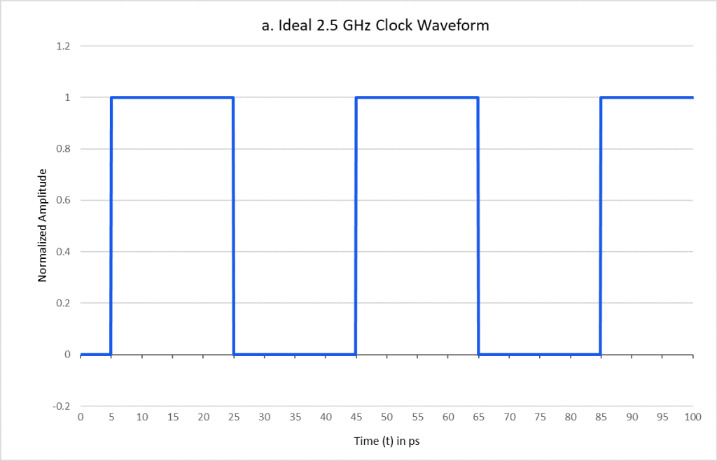
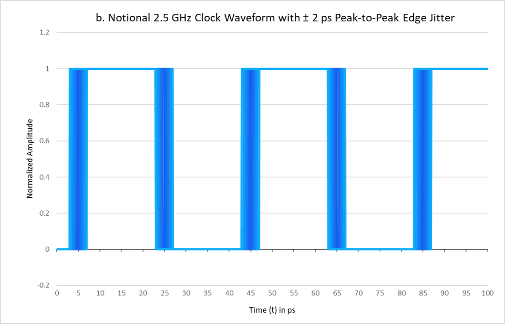
Figure 1: a. Ideal 2.5 GHz rectangular clock waveform and b. 2.5 GHz clock with ± 2 ps peak-to-peak (2.72 ps rms) of edge jitter.
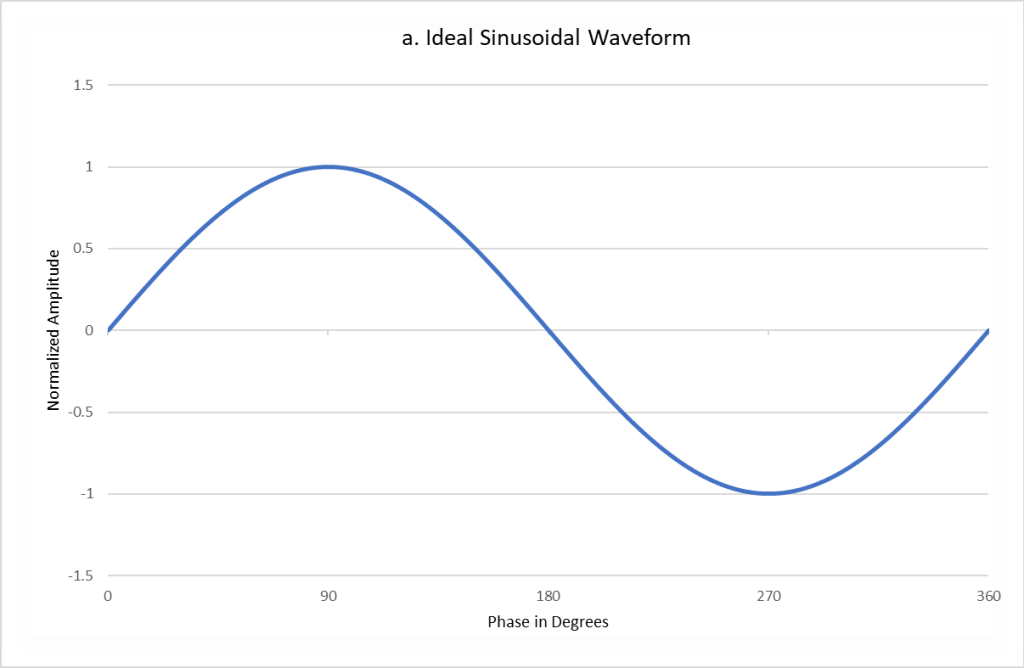
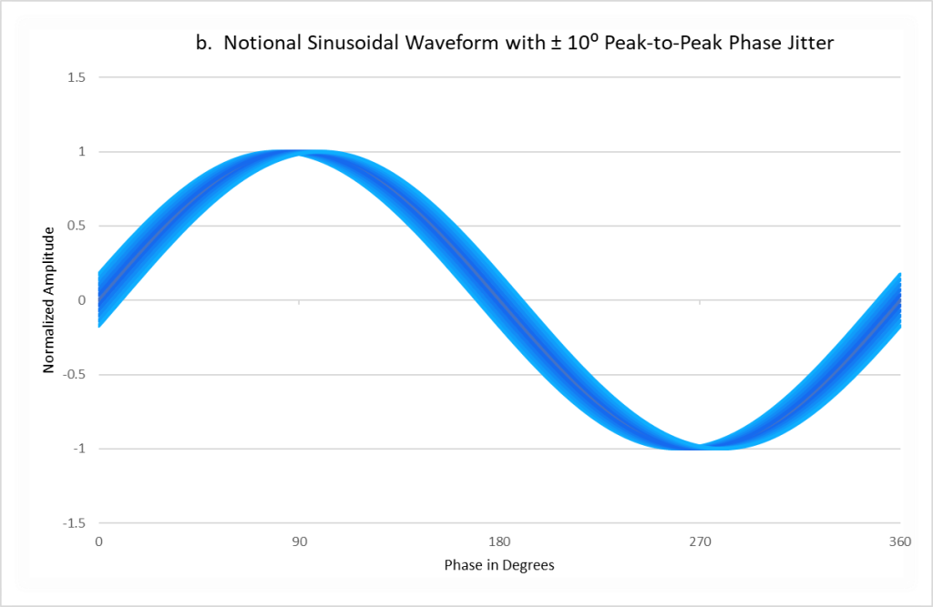
Figures 1b and 2b exhibit the time domain jitter of a rectangular wave and sine wave, respectively, though the scale of the jitter is greatly exaggerated (by more than an order of magnitude) for illustration purposes. Note that there are no amplitude fluctuations in either of these waveforms, such that purely phase jitter is present.
Single Sideband (SSB) Phase Noise and Spot Noise
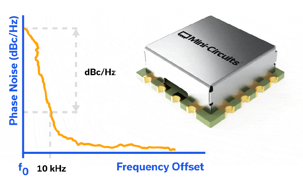
While phase jitter is interesting and will become an essential metric as we examine system performance, VCOs utilized for clock timing are rarely specified in terms of phase jitter. Instead, VCO performance is most often quantified by phase noise in the frequency domain. VCO phase noise is described as a power spectral density (in dBc/Hz) at each of several offsets from the center frequency, f0. Each of these values is referred to as a spot noise value. Figure 3 shows a single sideband (SSB) phase noise spectral plot with a single spot noise value of -120 dBc/Hz at 10 kHz offset from the carrier, f0. When highlighting component specifications, VCO manufacturers generally provide spot noise values for several offsets from the carrier frequency. Alternatively, a VCO can be characterized using a phase noise analyzer, or even a spectrum analyzer that has the appropriate measurement application. As VCOs are complex components, several more specifications – such as frequency pulling, frequency pushing, tuning sensitivity, drift, etc – are required to adequately define them. For more on VCO performance parameters, see this Glossary of VCO Terms, and for more on VCO test methods, refer to Mini-Circuits® VCO Test Methods.
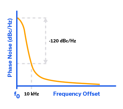
Understanding the phase noise power spectral density curve of a VCO is critical to understanding its impact on system performance. Unfortunately, the path from spot noise values in the frequency domain to rms phase jitter in the time domain, to system BER can be a circuitous one. The transition from the time domain to the frequency domain and back (i.e. from jitter to phase noise and back to jitter) is important to understand, but the explanation is lengthy and technical, so it has been included in Appendix A. Instead, we will focus on quickly determining integrated phase noise from a set of spot noise values and on how to convert this integrated phase noise value to rms jitter. In subsequent sections, we examine the effect of rms phase jitter on system BER for 256 QAM.
Spot Noise and Integrated Phase Noise
Mini-Circuits-provided spot noise values for three separate VCOs are shown in Table 1 for offset frequencies of 1 kHz, 10 kHz, 100 kHz and 1 MHz. A piecewise linear approximation on a log-log scale between these spot noise values is shown as the phase noise spectrum of Figure 4.
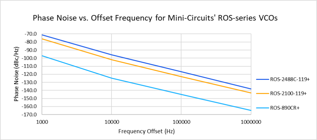
In order to calculate integrated phase noise from 1 kHz to 1 MHz, the area under the piecewise linear approximation for each of the three separate segments (1 kHz to 10 kHz, 10 kHz to 100 kHz, and 100 kHz to 1 MHz) is computed as in equation [10] and then summed and expressed in dBc as in [11] of Appendix A. Both equations are repeated below:


Using a typical Excel® spreadsheet, we can combine these calculations to determine integrated phase noise from 1 kHz to 1 MHz offset directly for the ROS-2488C-119+ VCO (row 4) using the equation below (refer to the notional column and row labeling outside the borders of Table 1 for cell references):
Integrated Phase Noise =10*LOG((10^(C4/10))*($C$2^(-(D4-C4)/10))*(((D4-C4)/10+1)^(-1))*($D$2^((D4-C4)/10+1)-$C$2^((D4-C4)/10+1))+(10^(D4/10))*($D$2^(-(E4-D4)/10))*(((E4-D4)/10+1)^(-1))*($E$2^((E4-D4)/10+1)-$D$2^((E4-D4)/10+1))+(10^(E4/10))*($E$2^(-(F4-E4)/10))*(((F4-E4)/10+1)^(-1))*($F$2^((F4-E4)/10+1)-$E$2^((F4-E4)/10+1))+(10^(F4/10))*($F$2^(-(I4-F4)/10))*(((I4-F4)/10 +1)^(-1))*($I$2^((I4-F4)/10 + 1) – $F$2^((I4-F4)/10+1))) [1]
The calculated values of integrated phase noise are shown in column G of Table 1 for each of the three VCOs. Integrated phase noise expressed in dBc across a specific band of offset frequencies is interesting, as it is the phase noise power relative to the carrier. Alternatively, changing the sign of the integrated phase noise gives us the signal-to-phase noise ratio in dB. But these figures are still in the frequency domain. To better assess the impact of VCO integrated phase noise on system performance (BER), we convert from units of dBc to ⁰RMS (phase jitter).
Time Domain Phase Jitter
The conversion from units of dBc to ⁰RMS is straightforward and can be performed utilizing the following equation:

Using Excel® as before we have the following equation for row four, column H of the spreadsheet to perform the conversion to ⁰RMS:
=180*SQRT(10^((G4+10*LOG(2))/10))/PI() [3]
This conversion to ⁰RMS is performed differently in Appendix A by means of equations [7], [12], [13], and [14] to give the reader a deeper appreciation for units that are in their linear form vs. in dB. Nevertheless, the results of this conversion are shown in column H of Table 1. The ROS-2488C-119+ has a phase jitter of 0.59⁰RMS, the ROS-2100-119+ clocks in at 0.32⁰RMS (pun intended), and the ROS-890CR+ an exceptional 0.027⁰RMS. While these may not seem like meaningful figures at a glance, rest assured that we’re one step closer to being able to assess system performance given this knowledge of VCO phase jitter. We have chosen 256 QAM since its phase jitter tolerance and constellations are readily available.
256 Quadrature Amplitude Modulation (QAM) BER for Multiple Phase Jitter Levels
256 QAM is a convenient modulation to utilize to draw a comparison of phase noise effects on system performance. While higher order M-ary QAM modulations are in broad use today, none lend themselves as well to examination and analysis as 256 QAM. From Table 1 we know the free running integrated phase noise and the associated RMS phase jitter for each of the three Mini-Circuits’ VCOs. Figure 5 shows, left-to-right, the BER vs. SNR (or Eb/No) curve for AWGN-only jitter, 0.25⁰RMS, 0.35⁰RMS, 0.5⁰RMS phase jitter.
Note that the scale of Eb/No and SNR are the same, merely offset by 10 log 8 = 9 dB, because 256-QAM contains eight bits per symbol.1
The effect of designing in the ROS-2100-119+ VCO (0.32⁰RMS) would result in system performance that closely matches that shown by the blue, dashed trace, and utilizing the ROS-2488C-119+ VCO (0.59⁰RMS), system performance approximated by the red, dashed trace. We see along the x-axis, that to achieve a BER of y=10-9, the SNR required for the ROS-2488C-119+ VCO is approximately 37.5 dB, and for the ROS-2100-119+ VCO, 35.5 dB. In telecommunications, a BER of 10-9 is acceptable, but for data transmission, BERs several orders of magnitude better are often required. Keep in mind that this is a very cursory, simplified analysis which considers all error to be untracked, and includes no error correction or other phase noise contributors.
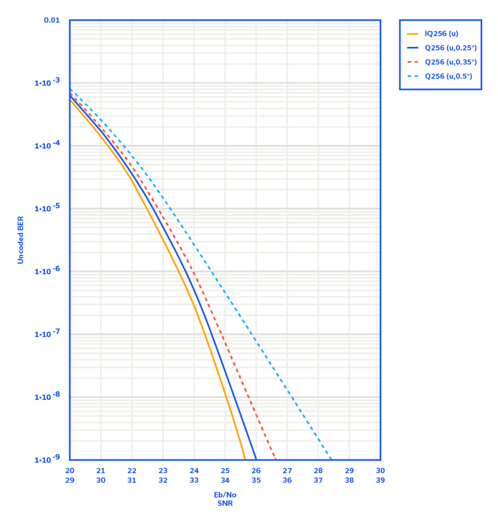
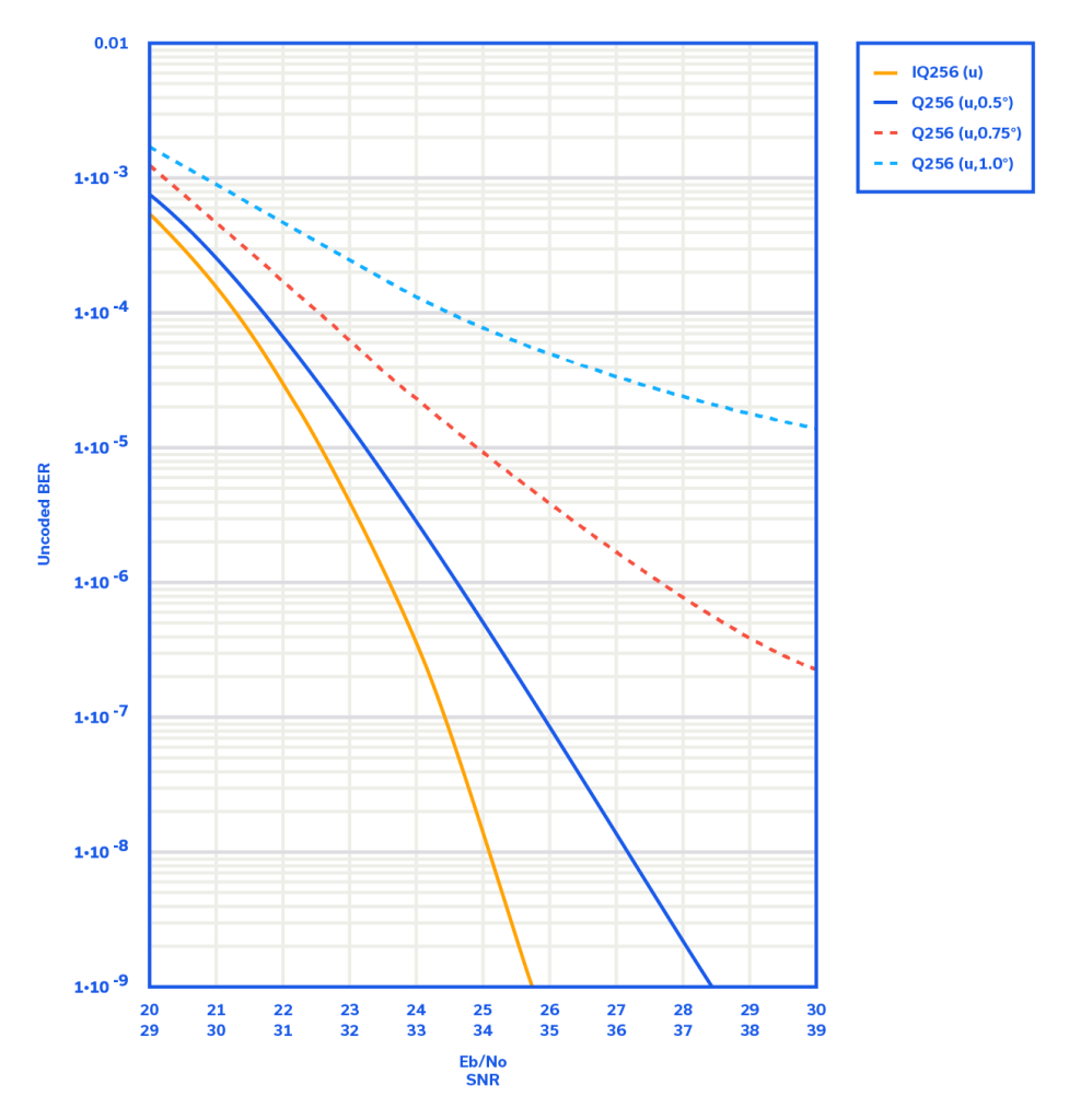
Figure 6 has been included for good measure to illustrate what happens to the BER curve as phase jitter continues to degrade beyond 0.5⁰RMS to 0.75⁰RMS and 1.0⁰RMS. Clearly reasonable BERs can no longer be achieved, even at elevated SNRs.
We have saved the best for last. The excellent phase noise performance of the ROS-890CR+ (0.027⁰RMS) is so low, that a system designed around this VCO would exhibit performance that closely approximates the additive white Gaussian noise (AWGN)-only curve in Figures 5 and 6. Higher order QAM modulation schemes (1024 QAM and 4096 QAM, for example) most often require exceptionally low phase noise clocks.
Note that we are utilizing phase jitter in units of ⁰RMS. These units can be converted to units of time, given an a priori knowledge of the carrier frequency, f0, as shown in Appendix A.
256 QAM Constellation Diagrams vs. Phase Jitter Level
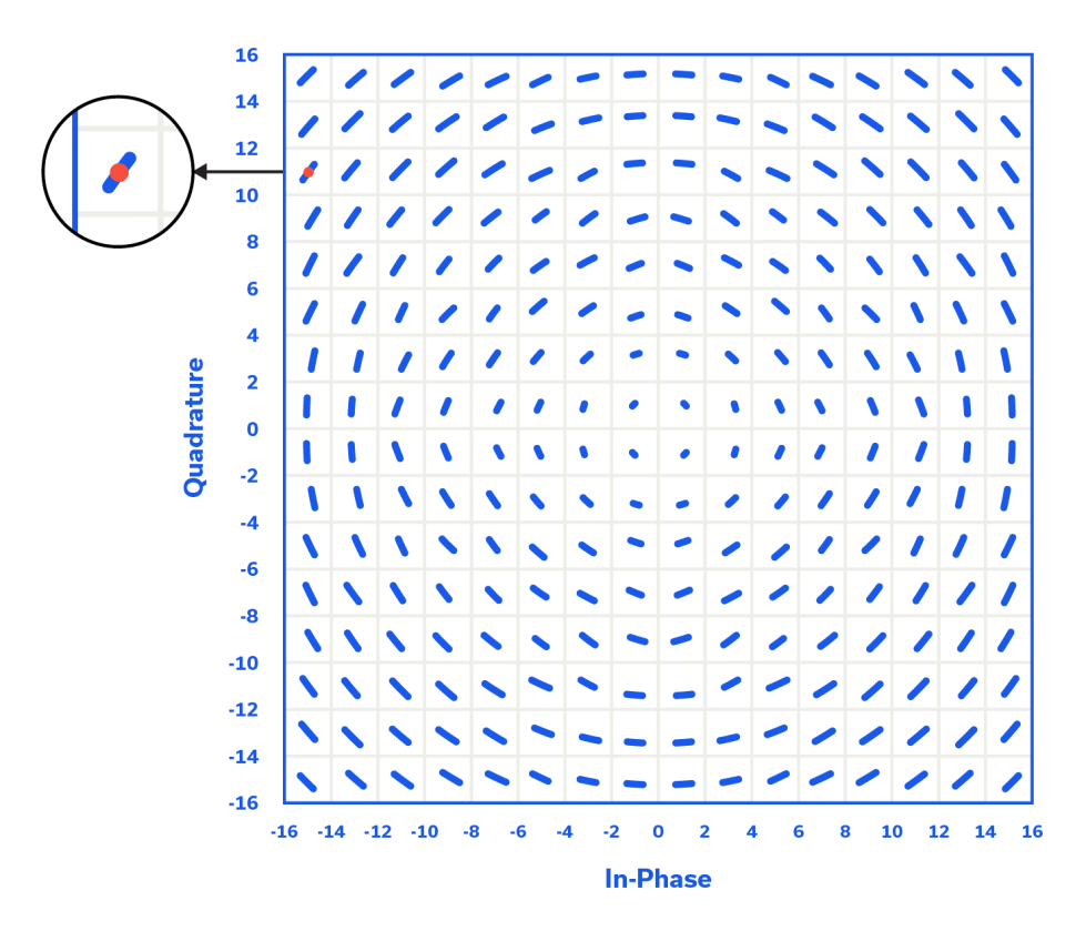
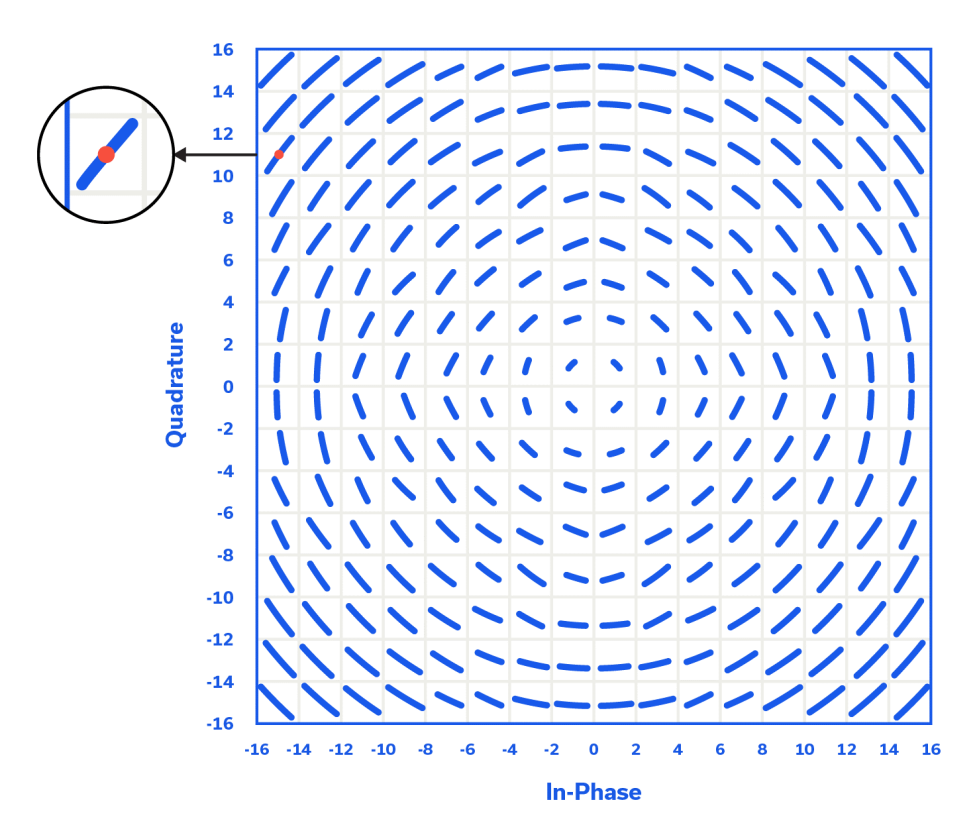
Figures 7 and 8 show notional 256-QAM constellation diagrams for phase jitter values of 0.5⁰RMS and greater than 1.0⁰RMS, respectively, and at an approximate SNR of 60 dB. The diagrams are similar insofar as the angular, Gaussian phase jitter becomes more pronounced for the outer symbols. However, for a greater magnitude of RMS phase jitter (>1.0⁰RMS vs. 0.5⁰RMS), significantly greater statistical, angular displacement drives the symbols (the outermost ones in particular) closer to the symbol boundaries, making it easier for AWGN to drive them into an adjacent symbol location, resulting in an increased BER. Moreover, the notional constellation diagram is a good method for qualitatively viewing the effect of different levels of phase jitter on system performance. The red dot in the symbol location of the inset for Figures 7 and 8 is designed to exhibit an SNR of 60 dB. While in reality this constellation point (symbol) would not be a well-defined dot (instead it would be clouded by AWGN 60 dB down from the carrier), the dot helps to illustrate how that symbol is angularly smeared by higher levels of phase noise, or in the case of Figure 7 approximately 0.5⁰RMS of phase jitter and for Figure 8 greater than 1.0⁰RMS.
Signal-to-Noise Ratio (SNR) and BER for 256 QAM
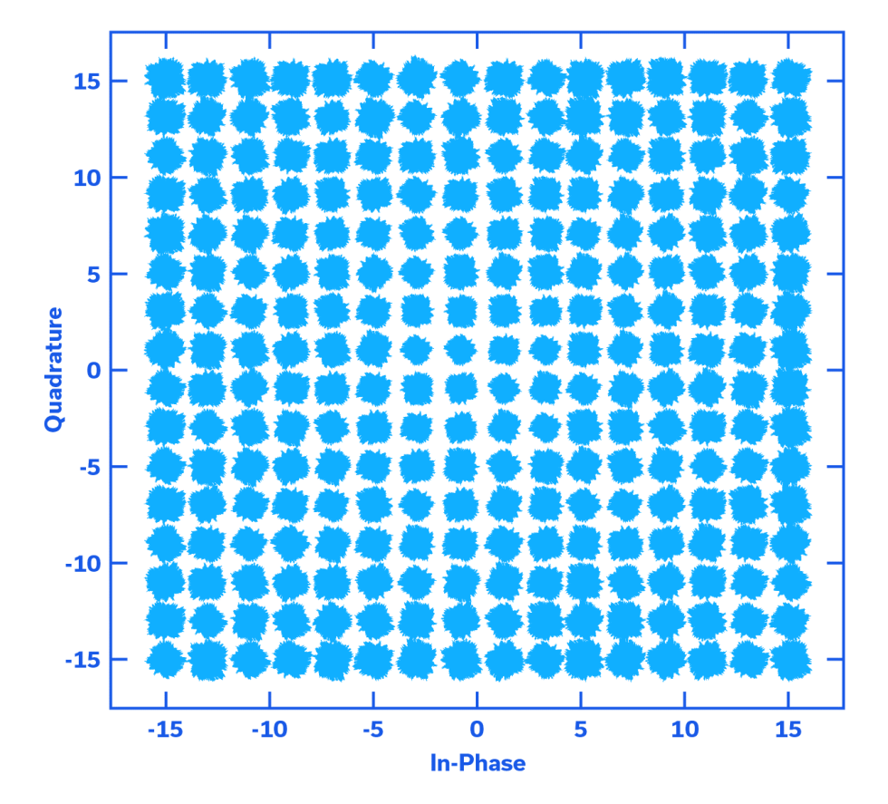
An SNR of 60 dB is very useful for depicting the effect of phase jitter on overall system performance, or for painting “thin” lines (symbols that are the result of a Gaussian distribution of angular rotations) on a constellation diagram, as in Figures 7 and 8. In the real world, however, an SNR of 60 dB is hard to come by, and not only does AWGN impact phase, but also amplitude (the radial distance from the origin on the constellation diagram to a given symbol). For good measure, it is worthwhile to examine the notional constellation diagram of Figure 9, modeled at an SNR of less than 30 dB. Clearly the phase jitter level must be greater than the 0.5⁰RMS shown in Figure 7, and perhaps greater than 1.0⁰RMS, as shown in Figure 8. The BER is not particularly good, as symbols, specifically the outermost symbols, can readily be driven beyond their boundaries. Figure 9 is a good example of a 256 QAM system being operated near its performance limits. One final observation that may not be apparent at a glance, is that, even in the presence of a higher level of AWGN, the outer symbols still exhibit greater statistical distribution than the more centrally-located symbols, which tend to look “tighter”.
Phased Out
In this application note we studied the time domain phenomenon known as jitter that gives rise to phase noise in the frequency domain. Once we began to examine phase noise, we also discussed briefly several other VCO specifications critical to VCO selection. We then took note of three specific Mini-Circuits’ VCOs and their spot noise specifications. From spot noise, we showed how to calculate integrated phase noise, and provided the reader an Excel® equation. The theoretical approach is included in Appendix A. Integrated phase noise was quickly converted to phase jitter in ⁰RMS, and phase jitter enabled us to examine 256 QAM system BER vs. SNR performance curves for several levels of phase jitter. The Mini-Circuits’ VCOs were applied to the system to determine the required SNR to achieve a BER of 10-9. We also analyzed notional 256 QAM constellation diagrams for 0.5⁰RMS and >1.0⁰RMS phase noise at 60 dB SNR to see the impact of additional phase noise on symbol quality. Finally, we reviewed a notional constellation diagram for a 256 QAM system operating at an SNR of <30 dB and an unspecified phase jitter, concluding that the system was being operated at the limits of its performance capabilities.
Appendix A – Phase Jitter and Phase Noise from the Time Domain to the Frequency Domain and Back
At the outset of this application note, phase jitter was conceptualized as zero crossing fluctuations for a sinusoidal waveform or as edge jitter for a square wave. When one thinks of phase noise, the frequency domain power spectral density curve centered at f0 immediately comes to mind. Phase noise is an alternative way of expressing phase jitter, the actual time domain phenomenon at the core of phase noise. So how do we get from phase jitter in the time domain, to phase noise in the frequency domain, to an integrated phase noise value and back to an RMS phase jitter figure? This appendix is designed to provide the reader a basic guide to the mathematical derivations involved in expressing phase jitter in the time domain, converting it to phase noise in the frequency domain, integrating phase noise over a specific range of offset (Fourier) frequencies, and expressing the integrated phase noise as RMS jitter. The main goal is to offer the designer a unique set of references to pursue for the mathematical derivations required for each step of the transition from the time domain to the frequency domain and back. Specifically, in the time domain, two references detail taking the Fourier transform of the autocorrelation of the discrete time random process (phase jitter sequence) to get to the frequency domain. Integral calculus is demonstrated to provide the area under a linear segment of a piecewise linear curve on a log-log scale. The designer can then compute the area under n sections and determine the integrated phase noise from a phase noise power spectral density curve, or from a set of spot noise values. Once integrated phase noise is determined, translation back to RMS phase jitter is quite straightforward. The overarching goal is to keep this application note succinct and focused, while steering those that wish to delve deeper into the derivation details toward excellent reference material.
Phase Jitter in the Time Domain
For most waveforms that we generate or encounter, we’re primarily concerned with periodicity, or the signal’s ability to repeat at an interval of exactly T0 over time. In the real world, T0 becomes the mean period, and transitions are spaced from that ideal (mean) period by the absolute jitter sequence τk.2 We can also express a sequence in radians such that:
After the addition of noise with a variance of σn2, an amplitude A, and a frequency ω0, the variance of absolute jitter sequence τk due to noise is then:
ϕτ2 = σn2/A2ω02 [5], where Aω0 in the denominator is the sinusoidal slope at the zero crossings.2
This variance expressed in radians is:
σϕ2 = ϕτ2(2π/T0)2 = σn2/A2 [6], since ω0 = 2π/T0
These are both time domain representations of the absolute jitter.
Time Domain to Frequency Domain
By taking the Fourier transform of the autocorrelation of either discrete time random process, we get a frequency domain representation of the absolute jitter. Taking the Fourier transform of the autocorrelation of the phase jitter random process, ϕk yields the phase noise power spectral density Sϕ(f) in rad2/Hz. For more inquisitive readers, Ali Sheikholeslami expands the concept of “excess phase” into the autocorrelation and determines the phase noise spectral density by taking its integral in his 2019 ESSCIRC presentation.3
In his graduate-level video series 30 Jitter and Phase Noise in Oscillators – YouTube2, between timestamps 29:35 and 38:40, Professor Tony Chan Carusone keeps excellent track of units while defining normalized (to the center frequency and to the carrier power (A2/2)) ℒ(f) in dBc/Hz where he uses ℒ(Δf) in lieu of ℒ(f).
Integration in the Frequency Domain
Phase noise has been well understood for a number of decades and, when an RF/analog designer specifies phase noise, invariably the frequency domain representation ℒ(f) expressed in units of dBc/Hz is what they refer to. As an aside, it’s interesting that ℒ(f) has become the gold standard for phase noise measurements, and is even defined in IEEE Standard 1139-19882. Rubiola and Vernotte, renowned experts with “over 30 years in the field” aren’t convinced that this is the optimal choice, and trace its origins to a 1964 IEEE/NASA symposium.4 The problem lies in the units of ℒ(f), and the single page referenced in [3] is a concise and informative read. Being a stickler for units, this author agrees with Rubiola and Vernotte. Nevertheless, ℒ(f) expressed in units of dBc/Hz will continue to be the standard measure of phase noise in the frequency domain going forward. Furthermore, ℒ(f) is directly related to Sϕ(f) by the equation2:
ℒ(f) = Sϕ(f)/2 for Sϕ(f)<<1 [7],
and where ℒ(f) is in normalized (linear) power/Hz and Sϕ(f) is in rad2/Hz.
We most often find a set of ℒ(f) spot noise values or an ℒ(f) curve plotted on a log-log scale in literature and on data sheets for components. A set of spot noise values can readily be interpreted as a piecewise linear function, and the curve may be approximated as piecewise linear as well, if it is not already provided in that form. How is integrated phase noise determined from a piecewise linear function ℒ(f) on a log-log scale? Most designers will answer by naming their favorite online phase noise calculator. While this is one possibility, it is more interesting to examine the math behind the integration process.
On page 21 of his work “Phase Noise Analysis and Basic Measuring Techniques”,5 Ferrell begins his example with a key ingredient, slope.5 On page 22, he clearly points out the conversion from log back to linear in order to perform the integration.5 This understanding of slope and the need to integrate linearly, taken in conjunction with the Wikipedia integration example6, and edited to incorporate the most common notation (m for slope, c for constant) give us:
ℒ(f) = cfm [8]
and for the integration between two frequency endpoints:

his result is for the area of one segment of a piecewise linear function (or one approximated to be so) on a log-log scale. Note that the units are still in linear, normalized power. If there are subsequent sections to be integrated, the results must be added together in linear units and the sum converted to logarithmic units (dBc) by taking:
10 log (A1 +A2 + A3 + … +An) [11]
This will yield a single figure in dBc that we call integrated phase noise, calculated over an f1 to fn offset frequency range. It is often difficult to appreciate the magnitude of a single figure in dBc across a range of offset frequencies. For instance, what performance level can be expected from an oscillator with an integrated phase noise across 100 Hz to 1 MHz of -40, -50, or -60 dBc? To solve this dilemma, we look back to the time domain.
Transformation Back to the Time Domain
Phase noise for a multitude of systems is often specified by its equivalent time domain phenomenon, phase jitter. The conversions between units of linear (normalized) power/Hz and rad2/Hz were previously shown from equation [7]to be quite simple from:
ℒ(f) = Sϕ(f)/2 [7],
and therefore: Sϕ(f) = 2 ℒ(f) (rad2/Hz) [12]
For the last equation to express Sϕ(f) in units of rad2/Hz, the units of ℒ(f) must be linear and not logarithmic. After this conversion, we simply take the square root of Sϕ(f) to obtain the resulting RMS phase jitter in radians:

Degrees RMS and seconds RMS are very common units by which phase jitter is specified. Many modern instruments enable a user to directly measure these values for a given RF carrier.
References
- 2001-the-exact-ber-performance-of-256-qam-with-rf-carrier-phase-noise
- Professor Tony Chan Carusone, one of a video series of graduate-level topics from his “Analog Integrated Circuit Design text, 30 Jitter and Phase Noise in Oscillators – YouTube 0:00-13:18 and 29:25-38:40
- Ali Sheikholeslami, ESSCIRC 2019 Tutorial: Jitter and Phase Noise, Fundamental Concepts in Jitter and Phase Noise Presented by Ali Sheikholeslami – YouTube, 1:00:00-1:12:30
- E. Rubiola and F. Vernotte, The Companion of Enrico’s Chart for Phase Noise and Two-Sample Variances, P. 6, https://arxiv.org/pdf/2201.07109.pdf
- James Alton Ferrell, Phase Noise Analysis and Basic Measuring Techniques, Summer Term 1988, Phase noise analysis and basic measuring techniques (ucf.edu), pp. 17-22
- Wikipedia, Finding the Area under a Straight-line Segment of Log-Log Plot, Log–log plot – Wikipedia
- Wenzel Associates, Inc., Spreadsheets/Programs, Allan Variance from Phase Noise (also calculates total RMS jitter over the specified bandwidth), March 23, 1998


