RF/Microwave Balanced Amplifiers and Their Applications

A balanced amplifier is the proper term for a pair of devices operated in quadrature phase and combined to amplify a signal. Quadrature simply means that signals incident upon the devices are 90⁰ out-of-phase with one another. The term “quadrature-combined pair” (often shortened to simply “quad-combined pair”) is perhaps just as common as “balanced amplifier,” and both are as identical as “PTFE” is to “Teflon®.”
This article explains the use of quadrature hybrid splitters and combiners (also often called hybrid couplers) in balanced amplifier configurations and the advantages of combining two amplifier devices in this fashion. Two of the most common applications for the balanced amplifier (quad-combined pair) are described by way of example.
Quadrature Hybrids: Splitting RF Signal with 90⁰ Phase Shifts
Quadrature hybrids have inherent -90⁰ phase shifts for each “leg” traversed by a signal, whether used as a power splitter (or “divider”) or as a combiner. An ideal quadrature hybrid will split the power of the RF input signal equally, applying half to each of two output ports, and delivering exactly zero power to the fourth, isolated port. Figure 1 shows a pair of amplifier devices nested between an input quadrature hybrid splitter (input “quad”) and an output quadrature hybrid combiner (output “quad”). As discussed previously, this entire structure, from RF In to RF Out is referred to as a balanced amplifier, or a quad-combined pair.

Looking at the quadrature hybrid schematic, each of the horizontal and vertical lengths between ports is referred to herein as a “leg.” Moving counterclockwise, the signal shifts -90˚ for each leg traversed to arrive at a given port. Therefore the lower output signal is shifted -90˚ (one leg counterclockwise from the input port), and the upper output signal is shifted -180˚ (two legs counterclockwise). Therefore, in the ideal, theoretical case, the signal incident on each amplifier is equal in magnitude and 90˚ out-of-phase with its counterpart. Notice what happens at the isolated port: The counterclockwise-travelling signal experiences a phase shift of -270⁰, or 3 legs to get there, whereas the clockwise-travelling signal needs only a single -90⁰ leg. The two signals are exactly 180⁰ out-of-phase, and perfectly cancel, such that no power is dissipated in the 50Ω termination resistor at the isolated port.
Recombining Balanced RF Output Signals
Thus far we have two amplifier devices operated 90⁰ out-of-phase and we must recombine their outputs in-phase. To do so, we essentially invert the process we performed when splitting the signal by orienting the hybrid in the opposite direction as shown in Figure 1. If it sounds too simple to be true, just examine the associated phase shifts.
The lower device operates at -90⁰ of phase shift from the input signal, and its output takes the long way back to the combined port, travelling another two legs counterclockwise (-180⁰) for a total phase shift of -270⁰. The output signal of the upper device, already operating at -180⁰ of phase shift, takes the short way home, just a single -90⁰ leg becoming incident on the combined port at -270⁰ as well. The two signals combine perfectly in phase, and the quad-combined pair operates at double the power output and double the IP3 (+3 dB) of either amplifier on its own. Once again, the signals incident at the isolated port are exactly 180⁰ out-of-phase and perfectly cancel, so no power is dissipated in the 50Ω termination resistor.
Low-Power Balanced Amplifier Application and the Input Port Advantage
One common application for the balanced amplifier is in the low noise amplifier (LNA) of a receiver front end. In addition to high linearity / OIP3 requirements, designers are intent on squeezing every tenth of a dB of noise figure out of their LNA. The tradeoff for the desired combination of linearity and noise figure performance, however, is degradation of the input return loss and VSWR of the device. It’s not uncommon to find broadband, sub-1 dB noise figure, >+40 dBm OIP3 LNA MMICs with input VSWRs in the neighborhood of 2:1. This problem becomes even more significant when LNAs are designed with discrete devices such as GaN MESFETs, for which the input impedance is inordinately low (i.e. exceptionally high VSWR). Utilizing a quad-combined pair of low-noise, high-IP3 amplifiers is a common technique for improving VSWR in LNA designs.
So far, everything we have discussed has assumed ideal, lossless quads, amplifiers perfectly matched to 50Ω and identical in insertion phase. In reality, we know these conditions are impossible and some signal reflection between stages is expected. As a thought experiment, examine the input to the amplifier devices in Figure 1 and pretend they are fully reflective (infinite VSWR). Where does the input signal go?
Starting at the bottom, the -90⁰ input of the lower device bounces straight back to the RF input. The reflected signal traverses one leg in the clockwise direction and therefore experiences another -90⁰ of phase shift for a total of -180⁰ at the RF input port. Likewise, the upper device reflects its input signal back to the RF input with an additional -180 of phase shift, for a total phase angle of -360⁰. The two reflected wavefronts are 180⁰ out-of-phase at the RF input and cancel, effectively eliminating the effects impedance mismatch at the amplifier inputs. The reflected signals are fully in-phase and combine at the isolated port, but the combined power is dissipated in the 50Ω termination resistor, again with no effect upstream.
This means that the balanced amplifier not only doubles the total power output and IP3 of either amplifier alone, but also buffers the rest of the circuit from reflective elements commonly seen in discrete amplifiers with low noise and high IP3 performance. There are many other practical considerations such as whether the insertion loss of the hybrid is low enough to have only a modest impact on noise figure and whether the mismatch loss of running a 50Ω hybrid into a poorly matched device is worth the input VSWR stabilization. But overall, the high-linearity, low-noise, quad-combined pair is a proven technique for designing high-performance LNAs that has been widely used by circuit designers for decades.
Buffering Output Mismatch and Load Impedance Variations
Our emphasis to this point has been on the -90⁰ phase shifts that occur in the hybrid, enabling phase cancellation or in-phase combination, and the benefits these attributes offer for LNA design. But beyond the improvements in noise figure, IP3, and output power, quad-combined-pairs are remarkably effective at improving system performance anywhere a system connects to an imperfect load.

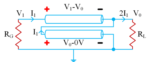
Figure 2 shows the phase shifts that a wavefront fully reflected from the output would experience, assuming an initial phase shift at the RF input port of 0⁰. Initially, the reflected signal traverses the quad and is incident upon the amplifier outputs at -90⁰ for the thru path (upper device) and -180⁰ for the coupled path (lower device). Note that the upper phase shifts correspond to the upper device and the lower phase shifts correspond to the lower device in the figure. Once the respective reflected signals hit the associated amplifier, they will reflect once again towards the output. The signals reflected off the internal devices are exactly 180⁰ out-of-phase at the RF output port, the upper device’s reflection at 180⁰ and the lower device’s reflection at 360⁰. This cancelling of the reflected signals is very similar to the input VSWR effect discussed previously. Finally, the signal first reflected off the load, then the internal devices combines in-phase at the termination resistor. Naturally this resistor must be sized appropriately.
In essence the RF output port of the quad-combined amplifier exhibits an excellent output VSWR because, looking back into the RF output from the load, there is theoretically no power reflected off the devices (VSWR = 1:1). Practically we know this isn’t possible for a multitude of reasons, but the effect of quadrature combining is pronounced, and the output VSWR of a quad-combined pair can be improved over that of a single device and stabilized against load impedance variations.
Summary
Because balanced amplifiers can be complex to analyze mathematically, this application note focused on providing a conceptual overview to make the basic theory of their operation accessible. The advantages of configuring a pair of amplifiers in quadrature and recombining them are many. This article discussed only the theoretically ideal case, and while practical considerations may often limit the performance of this quadrature-combined configuration, it is still a valuable tool in the designer’s arsenal for a variety of use cases.
Mini-Circuits’ wide selection of LTCC and MMIC 90˚ hybrids are popular for balanced amplifier configurations. We also offer a series of dual-matched MMIC amplifiers for both 50 and 75Ω impedance environments, which combine two matched amplifier die in a single, tiny QFN package. Combined with the aforementioned quads, these devices are a great solution to save space and simplify board layouts for balanced amplifier implementations.