Optimizing Transistor Stages for Different Operating Bandwidths
Since their invention by John Bardeen, Walter Brattain and William Shockley at Bell Labs in 1947, transistors have become a defining (if not the defining) feature of the contemporary technology landscape. Electric vehicles can have over 5 billion transistors in a given build, and today’s smartphones more than 10 billion! While their most common and familiar uses reside in the digital world, transistors are an essential element in RF circuits and systems, and while often integrated into more complex, multi-function devices, the simple transistor is still an essential tool in the designer’s toolkit.
Considering the expansive range of MMIC amplifiers now available on the market with integrated matching and bias circuitry, it can be easy to overlook the flexibility and economy of a discrete transistor solution. Perhaps your application requires that the gain roll off occur outside of the band of interest. Maybe the design is for a fiercely competitive, high-volume bid, and you don’t want to cough up four or five times the cost to achieve the same amplification with an internally matched MMIC.
Call it old school, but applying an RF/microwave transistor to the task of amplification is as tried and true a technique as they come. Often, the same transistor can be utilized in a variety of different ways depending on the peripheral circuitry utilized by the designer. More specifically, discrete transistors give designers the ability to design their own matching circuits and optimize characteristic performance for their exact application bandwidth.
This brief application note describes narrowband and broadband use cases for the same Mini-Circuits E-pHEMT transistor, the SAV-541+ as a demonstration of the versatility this simple device can provide. The compromises and tradeoffs in transitioning from narrowband to broadband implementation are discussed. Finally, a more integrated amplifier module (TAMP-1521GLN+) is discussed in detail to show the performance that can be achieved by cascading transistors.
Use Case #1: SAV-541+ E-pHEMT in a Narrowband Application
Figure 1 shows the schematic of an amplifier that utilizes the Mini-Circuits SAV-541+ E-pHEMT transistor as a gain stage. HEMTs generally have high gain, high switching speeds, and very low noise, which makes them useful in many microwave applications, especially in amplifiers.1 A prior article on pHEMT technology explores the underlying physics, fabrication process and related devices in greater detail.2
This model is specified for operation anywhere from 45 MHz to 6 GHz, and specifications are provided on the datasheet for different frequencies under certain operating conditions. As discussed, the actual performance in the user’s application will depend on the specific implementation. Let’s start by examining an application circuit for SAV-541+ in a narrowband low noise amplifier used in a customer’s system. The band of interest for this design is 2300 to 2400 MHz, which corresponds to the 5G n40 band (mirroring the 4G B40 band) in 3GPP Release 15.3
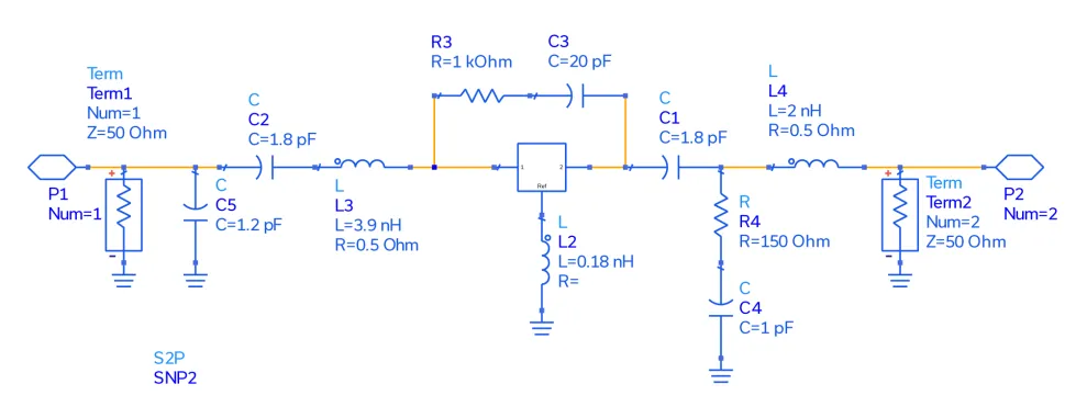
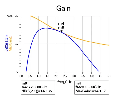
Note the source inductance, which is utilized to enhance stability and can be implemented with a simple 0Ω resistor R4, and the modest drain-to-gate negative feedback effected by the 1 kΩ resistor R3. A simulation of the gain (S21) for this circuit is shown in Figure 2. Gain north of 14 dB in the band of interest is quite good for a single-transistor amplifier.
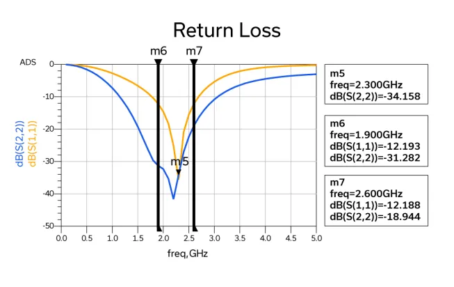
The input and output return loss (S11 and S22, respectively) are shown in Figure 3. The input return loss is 12 dB or better from 1900 to 2600 MHz and the output return loss is clearly greater than 20 dB over the 2300 to 2400 MHz band of interest.
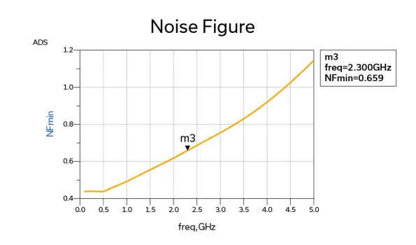
Noise figure (NF) performance for this band-optimized implementation is perhaps most impressive. Figure 4 shows a simulation with NF of just 0.659 dB at 2300 MHz, and less than 0.7 dB across the full 2300 to 2400 MHz band of interest. Consequently, the SAV-541+ would be suitable in this configuration as a gain element in an LNA for a sensitive receiver in the 5G n40 band.
Use Case #2: Broadening Bandwidth for the SAV-541+
We’ve established the potential performance of the SAV-541+ transistor in an application circuit optimized for a relatively narrow bandwidth. While design effort and board layout are obviously more complex with the discrete transistor approach than with a drop-in MMIC solution, the experienced designer can develop a matching network to extend the performance of this simple device for a wide variety of applications.
The schematic in Figure 5 shows a broadband application circuit for the SAV-541+ transistor. By comparison with the narrowband schematic in Figure 1, notice the relative dearth of the narrowband capacitive and inductive tuning elements in the single-digit pF and nH range, respectively. Additionally, notice the addition of the 8.2Ω resistive elements, utilized predominantly to ensure stability over the broader bandwidth. Finally, and perhaps most importantly, the drain-to-gate feedback resistor is now just one quarter the resistance of its counterpart in the narrowband application (240Ω vs. 1 kΩ). The stronger negative (parallel) feedback provided by the 240Ω resistor tends to broaden the bandwidth while reducing the gain. The easiest way to envision this effect is to assume that the one-stage, depletion mode device (pHEMT) has a constant gain-bandwidth product (GBWP) that declines log-linearly out to fT. Stronger drain-to-gate feedback, while reducing the gain, extends the bandwidth. This technique has been utilized by amplifier designers for many decades. Feedback can also be utilized to enhance stability, improve matching and to equalize (or “tilt”) the gain response.
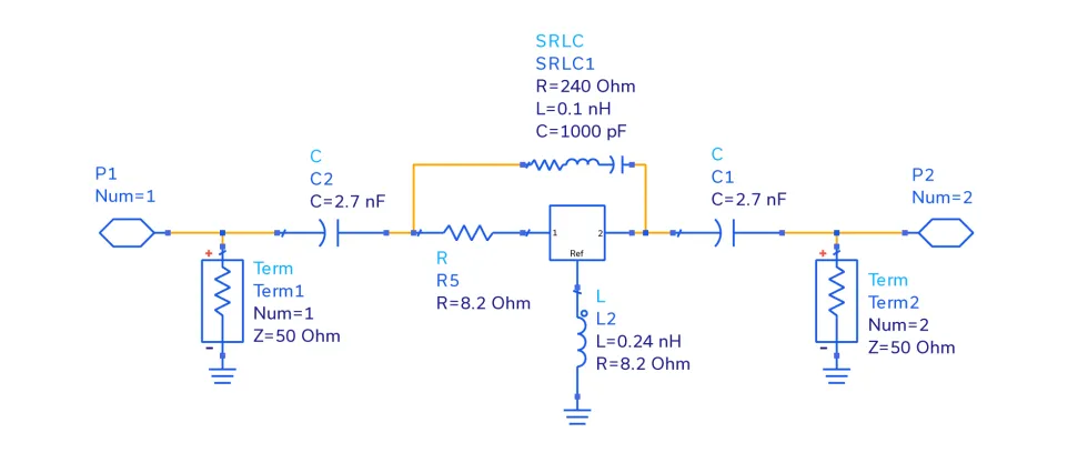
Figure 6 shows the simulated gain response for the broadband SAV-541+ amplifier circuit over the 5:1 bandwidth of 500 to 2500 MHz. It is immediately apparent that at least one compromise has been made to achieve such a broad bandwidth, as it comes at the expense of gain, which has decreased from 14 dB in the narrowband case to 11 dB in this configuration.
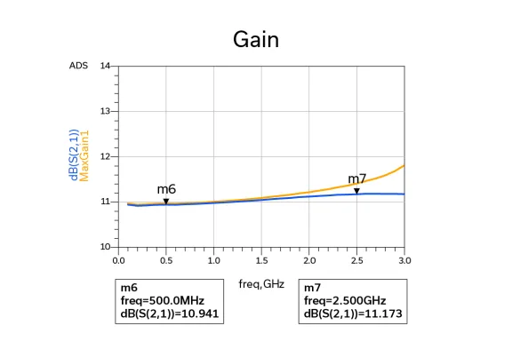
Notice how flat the gain response is across the 500 to 2500 MHz band (little more than a couple tenths of a dB). This is again the result of strong negative feedback, and an effect used by broadband power amplifier designers for many decades.
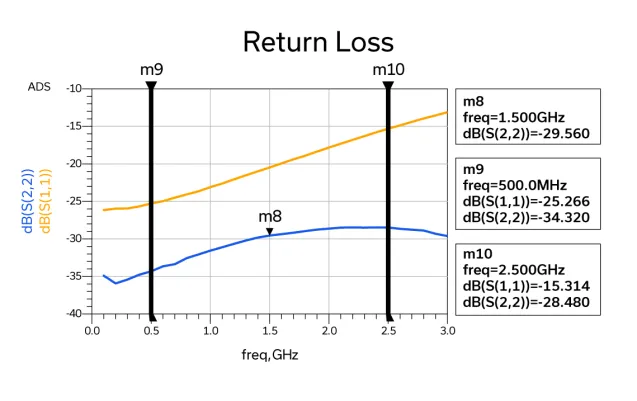
Both input and output return loss (S11 and S22, respectively) have remained excellent across the broader bandwidth as shown in Figure 7, with S11 spanning 16 to 25 dB and S22 ranging from about 28 to 33 dB. This is particularly good broadband matching for a low noise transistor.
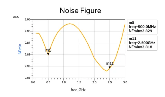
The simulated noise figure (NF) of the broadband implementation of SAV-541+ is shown in Figure 8, and while it appears to have a great deal of slope, notice that the y-axis scale is 0.01 dB per division. Compared to the narrowband circuit where the NF was less than 0.7 dB, the 2.85 dB level is quite an increase. Unfortunately, the bandwidth expansion achieved by feeding back more of the output (drain) to the input (gate) also entails feeding back more noise. Although a compromise of just over 2 dB was made to NF in order to achieve a 5:1 bandwidth, 2.85 dB is still very good noise performance, and a stage this broadband and with such excellent input/output return loss and gain flatness can find its way into many applications.
Multiple E-pHEMT Devices in Cascade
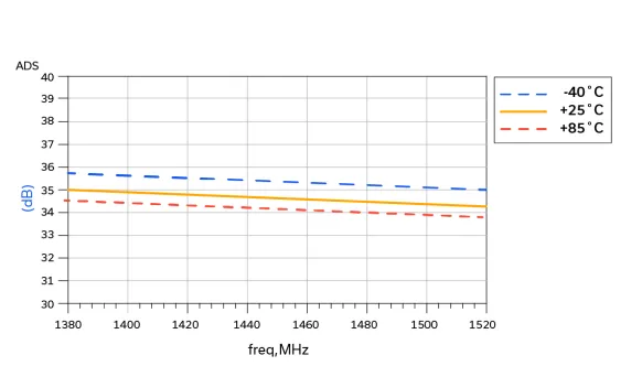
It’s common knowledge that cascading multiple transistors increases gain. This is exactly the technique used to design Mini-Circuits’ TAMP-1521GLN+ drop-in amplifier. A look under the hood of this integrated component reveals two stages that utilize the SAV-551+ E-pHEMT, a lower-current cousin of the SAV-541+, along with integrated biasing, matching and stability circuitry in a single, self-contained module (0.591” x 0.394” x 0.118”). The resulting performance is remarkable over the 1380 to 1520 MHz band, as shown in Figure 9. The narrowband performance shows 34 to 35 dB of gain with roughly ±1 dB flatness. Combining this gain performance with a typical NF 0.6 dB at room temperature makes the amplifier an outstanding ultra-low noise gain stage for its specified operating frequency range.
Application Flexibility
In this application note, we first presented an application circuit for the SAV-541+ optimized for the 2300 to 2400 band. Next, we showed an alternative circuit utilizing a different stabilization technique as well as negative feedback to achieve 20 times the bandwidth of the original circuit (500 to 2500 MHz). We then discussed the various tradeoffs of changing the feedback resistance to expand bandwidth, namely moderate sacrifices in gain and noise figure. Finally, we looked at the performance of the TAMP-1521GLN+ drop-in amplifier by way of example to demonstrate the performance of two cascaded E-pHEMTs optimized for a specific application bandwidth. Note as an extension that broadband stages utilizing stronger feedback can be cascaded in the same way.
Mini-Circuits’ SAV-541+ E-pHEMT and any of our discrete E-pHEMTs are available from stock in 4-lead SOT-343, 3x3mm, 2x2mm and 1.4×1.2mm QFN-style packages as well as bare die. These discrete E-pHEMT transistor circuits are very flexible, and can be optimized to achieve a variety of performance goals. Designers interested in using Mini-Circuits transistors for specific design goals can reach out to Mini-Circuits’ Applications Engineering team for implementation support.


