Exploring the Fundamentals of Thin-Film Filter Technology in RF & Microwave Applications
Finding the right filter for frequency ranges above the 3 GHz range is a perennial challenge for RF system engineers. Designers are typically looking for repeatable performance at production volume and a small, surface-mount form factor robust enough to withstand reflow onto their existing printed wiring board (PWB). Lumped element filters utilizing discrete wire-wound inductors and chip capacitors meet these criteria handily for passbands below about 3 GHz, but frequency response becomes more sensitive to variations in the physical structure of the device and temperature at higher frequencies, rendering this approach impractical.
Several filter technologies support application bands higher into the microwave range, but each comes with compromises, some of which may be non-starters for real-world system requirements. Suspended substrate stripline and cavity filters, for example achieve passbands up to around 40 GHz with outstanding rejection and selectivity, but they’re big, heavy and expensive. Also, because these are not surface-mount technologies, using them with integrated microwave assemblies requires launching the signal off the board to the connectorized filter interface and back onto the board, which adds loss and mismatch at the transitions. This is rarely viable.
Integrating the filter directly onto the PWB in the form inductor-capacitor pairs (L-C) in the conductive traces is one economical choice, and this might serve the engineer well for filtering a discrete signal as in an LO chain, for instance. When it comes to filtering complex waveforms in modulated or broadband signals, however, the band of interest and the filter requirements are often defined by a specified filter mask. In these applications, an on-board filter comprised of etched copper traces will struggle with performance and repeatability at higher frequencies. Most filters constructed using chemical etching processes will be limited in their repeatability due to tolerances inherent to the etching process. This technique sacrifices precious board space as typical PWB dielectric constants are not particularly high, rendering on-board filters larger than a discrete filter component.
Thin film filter technology is one solution for addressing these design concerns. Their high-accuracy fabrication process provides excellent repeatability, and ceramic substrates make for rugged construction and easy reflow onto existing PWBs. Some ceramic substrates exhibit high Dk characteristics, enabling very compact physical filter realizations. Thin film filters built on ceramic substrates are naturally temperature-stable over a broad operating temperature range. These filters exhibit a variety of performance characteristics that make them unique among other surface mount filter technologies including wide passband width up to 40 GHz, outstanding Q-factor, high power handling and rejection floor on the order of -60 dB and deeper.
The Thin-Film Filter Fabrication Process
RF thin film filters are typically fabricated by depositing thin layers of metal or dielectric material onto a substrate using a technique known as Physical Vapor Deposition (PVD), or sputtering. Sputtering utilizes plasma, usually generated from a gas such as Argon to deposit material from a target a few atoms at a time and onto a host substrate in specific pattern and thickness (from fractions of a nanometer to several micrometers). The thickness of each layer, the materials and the patterns utilized are carefully controlled to create the desired filter characteristics such as passband, selectivity, insertion loss, and rejection. These methods achieve extremely tight tolerances for material thickness and trace width. The benefit of processing filters using these sputtering techniques is shown in Figure 1, where the trace edges exhibit far superior uniformity for the filter processed using ion bean etching.1
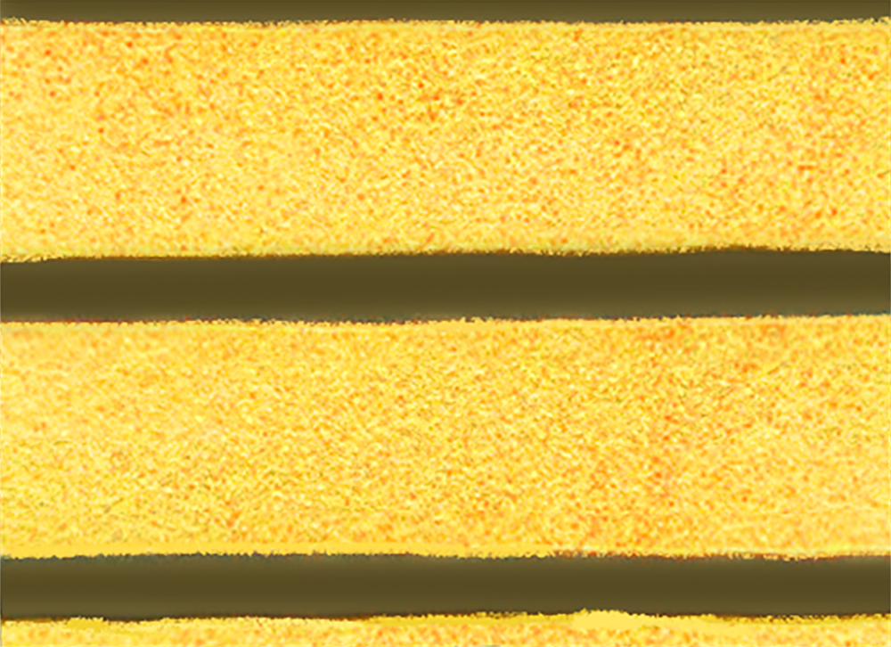

Figure 1: Chemically etched (left) vs. PVD fabricated (right) trace detail showing high precision of the sputtering process.
Thin-film technology can be used to realize a variety of filter topologies such as Bessel and Chebyshev and elliptic, response (e.g. band pass, low pass, high pass) and physical implementations like edge-coupled, hairpin, interdigitated and more. They are typically small compared to most filter technologies of similar performance and suitable for surface-mount assembly.
Common Applications
Thin film filter technology meets requirements for many applications from 3 GHz through mmWave where small device size and sharp rejection are both required. Mini-Circuits’ thin-film filters achieve very small form factors through the choice of high Dk materials and innovative implementations. Offering low passband insertion loss, steep rejection skirts, and wide stopband performance with designs over the DC to 40 GHz frequency range, thin-film filters are a cost-effective option compared to other options with comparable RF performance.
RF/microwave thin film filters are used in a wide range of applications, including wireless telecommunications (including 5G), satellite communications, traditional radar systems and mmWave radar, Internet of Things (IoT) and mmWave communications. They are known for their high performance, temperature stability, volumetric efficiency and high reliability in high-frequency environments.
Mini Circuits’ ABF-series of Thin-Film Filters
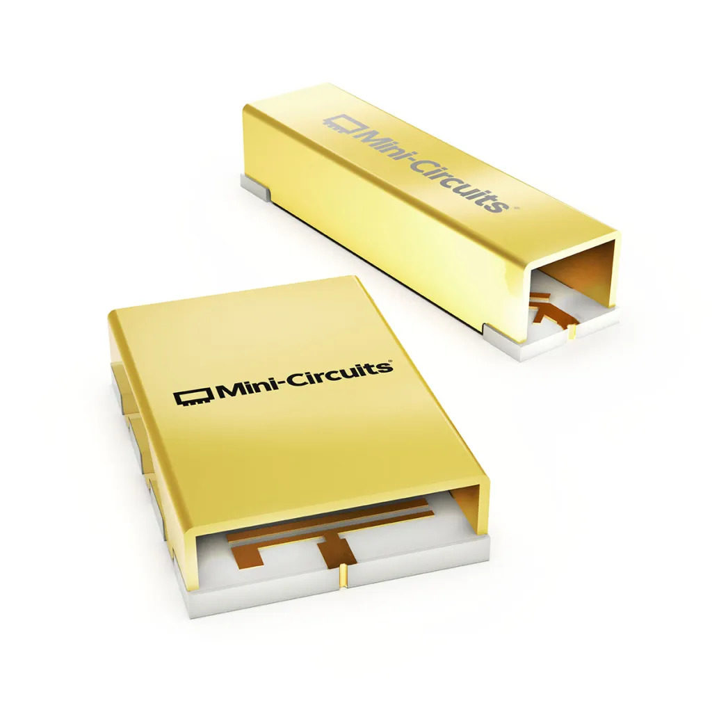
The ABF-series of filters from Mini-Circuits boasts very stable performance over a temperature range of -55⁰C to +125⁰C and is compatible with surface-mount reflow soldering techniques. As shown in Figure 2, the ABF filters incorporate a metal lid for shielding into the design. This feature enables simulations to be conducted that are much more accurate by confining the electromagnetic fields to within the filter structure, it avoids electromagnetic interaction with other components in the system, and it provides a surface that can be placed in close contact with the system housing structure to ensure excellent isolation.
Mini-Circuits’ selection of thin film on alumina bandpass filters exhibits impressive combinations of performance and size. As an example, Figure 3 shows the insertion loss and return loss for the ABF-26G+, a bandpass filter centered at 25.875 GHz designed to cover the 5G n258 band (24.25 to 27.5 GHz). Mid-band insertion loss measures less than 1.5 dB, and the return loss achieves nearly 20 dB across the entire band.
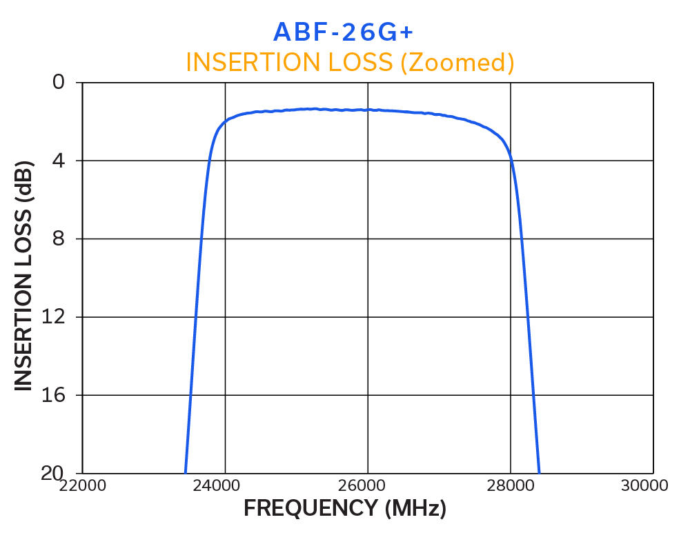
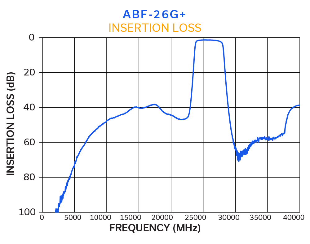
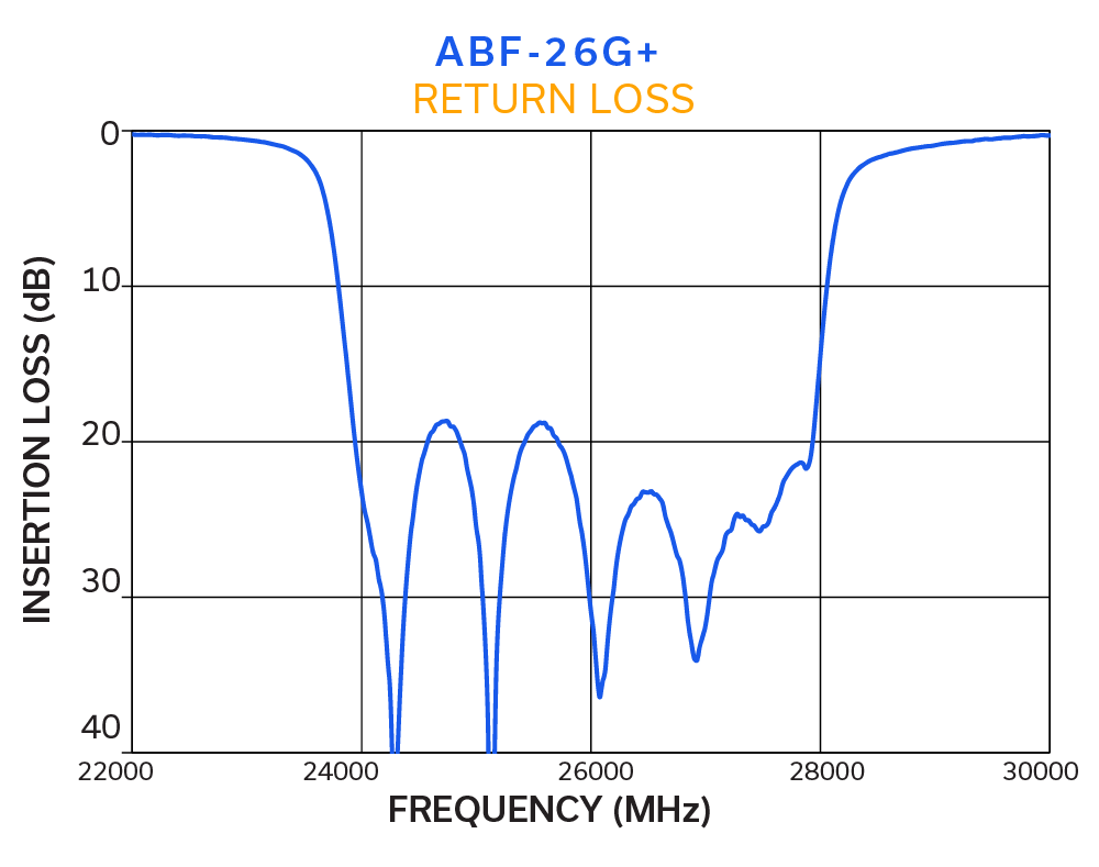
Figure 3: Insertion loss and return loss performance of an ABF-26G+ thin film band pass filter for the 5G n258 band
Another example from the ABF-series is the ABF-7R75G+ thin-film bandpass filter, centered at a frequency of 7.75 GHz. Figure 5 shows that this filter utilizes an innovative architecture to achieve a bandwidth of approximately 50% with an insertion loss of less than 1.5 dB across the band. This performance is achieved in a package footprint that measures just 0.07 in2 (45.45mm2), as shown in Figure 4.
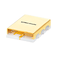
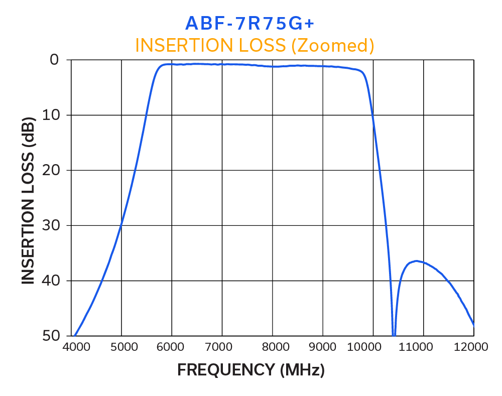
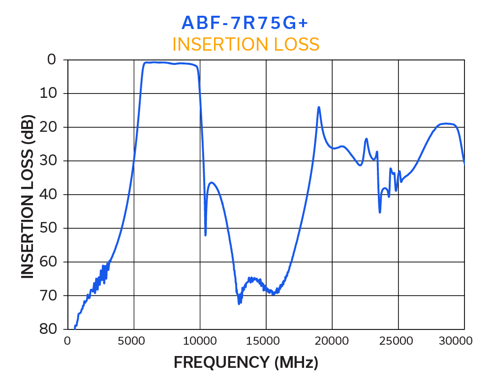
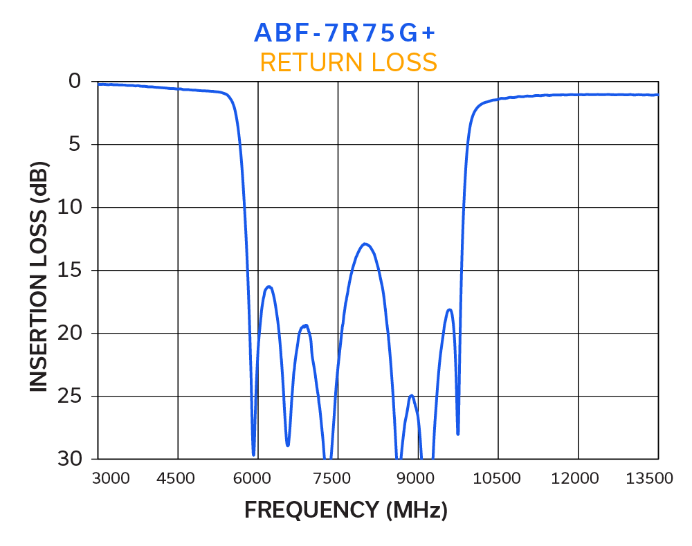
Figure 5: Insertion loss and return loss performance for an ABF-7R75G+ thin film band pass filter centered at 7.75 GHz
The Skinny on Thin-Film Filters
Thin-film filter technology affords the RF systems engineer many benefits such as low insertion loss, high rejection, good power handling, wide temperature range, excellent temperature stability, and repeatability. These attributes combined with their small size and surface-mount form factors makes these filters an excellent solution for many systems where high-Q is required but space is at a premium. Longstanding, precision processing techniques make the realization of many innovative architectures possible at scale with thin film.

Explore Mini-Circuits’ Full Thin-Film Filter Selection
- Passbands from 6.3 to 29.5 GHz
- Wide stopbands up to 40 GHz
- Fast roll-off
- Small, SMT package styles
- Custom designs available


