

Distributed RF Amplifier Designs for Ultra-Wideband Applications
Anirudh Venkatesan, Mini-Circuits Engineering
Amplifiers are used in RF systems to boost the power level of a signal. Conventional RF amplifiers are designed using reactive elements to achieve matching to the characteristic impedance of a circuit within the specified operating frequency range for a given system. Reactively matched amplifiers allow designers to optimize performance parameters for a broad range of system requirements. Combined with techniques like balancing, using 90˚ hybrids and negative feedback, they can support bandwidths as wide as about 10:1.
However, some ultra-wideband applications such as electronic warfare (EW), C through Q-Band SatCom and fiberoptic networks, may require instantaneous bandwidth on the order of 50 GHz or more in some cases, and thus come up against bandwidth limitations inherent to reactively matched designs. In such cases, distributed amplifier architectures provide one solution for covering multi-decade frequency range with a single device while offering perhaps the best all-around combination of gain flatness, noise figure, OIP3 and other key parameters. Distributed designs are also less susceptible to process variation resulting in excellent repeatability.
This article will review some of the differences between reactively matched and distributed amplifier designs. Distributed amplifier architectures will be presented and reviewed in particular detail, and examples of distributed amplifiers from Mini-Circuits’ MMIC product line will be given for illustration.
Reactively Matched Amplifiers
Figure 1 shows a typical, reactively-matched amplifier architecture:

Once a transistor is biased and stabilized, it needs to be matched. In typical applications, RF amplifiers are used in either a 50Ω or 75Ω environment. The transistors, however, do not have 50Ω or 75Ω impedances at their input and output. These mismatches will degrade the return losses of the amplifier, which means maximum available power gain cannot be achieved.
For example, when designing a reactively matched low noise amplifier, first the optimal input impedance is selected. This is done by utilizing noise figure and gain circles on the source reflection plane. Figure 2 below shows an example of the circles and the chosen point, which we shall now define as ГS.

Next, the output reflection coefficient of the transistor is calculated using the following equation:

After calculating ГOUT, we can design our output matching network to be the conjugate of ГOUT. In this case, the input is not conjugately matched because it was matched for the best combination of gain and noise figure.
An amplifier can also be simultaneously conjugately matched at the input and the output if the necessary stability condition of k>1 is satisfied. Here, k is calculated using the following equation:

The simultaneous conjugate matching at the input and the output is usually an iterative process as any non-zero S12 will cause a change in impedance at the input if the output match is changed and vice versa.
One drawback of this technique is that matching networks are inherently band limited. This means that the desired performance is achieved for a fractional bandwidth of about 10 to 30%. However, there are techniques to significantly increase the bandwidth of these amplifiers. Reactive matching networks with 90˚ hybrids on the input and output can achieve upwards of 3:1 bandwidth. Adding negative feedback can increase the bandwidths to the order of 10:1. Many Mini-Circuits MMIC amplifier designs utilize reactive matching with negative feedback to cover full-decade bandwidths. Some MMIC amplifiers from Mini-Circuits that use traditional matching are PMA2-153LN+, TSS-183A+ and EHC-24L+ which come in package sizes as small as 3×3 mm.
MMIC amplifiers from Mini-Circuits that use traditional matching
| Model No. | Freq. Range (GHz) | Gain (dB) | Noise Figure (dB) | OIP3 (dBm) | P1dB (dBm) |
| EHC-24L+ | DC-20 | 12.8 | 5.3 | 12.8 | 4.4 |
| TSS-183A+ | 5-18 | 13.6 | 4.6 | 27.8 | 17.8 |
| PMA2-153LN+ | 0.5-15 | 16 | 2.6 | 28 | 14.8 |
If wider bandwidths are needed, distributed MMIC amplifier design techniques can be used.
Distributed Amplifiers
With the increasing demand for broader bandwidths, distributed MMIC amplifier design techniques offer one way to satisfy requirements for good overall performance over multi-decade bandwidths.
In a distributed amplifier, broadband match is achieved on the input by absorbing the intrinsic gate-source capacitance (CGS) of the transistor into an artificial transmission line structure called “gate line.” Similarly, for the output, the intrinsic drain-source capacitance (CDS) is absorbed into another transmission line structure, named “drain line.” This creates a low pass structure that allows for a wideband response.
A basic distributed amplifier architecture using common source FETs is illustrated below in Figure 3:

The gate and drain lines are designed to have a wide bandwidth. The transistor is selected so that it has a high fmax. This allows for the design of very wideband amplifiers.
Let us consider the first section of the above architecture. Since for FETs the CGS is higher than the CDS, this is what will determine the cutoff frequency of the amplifier. For a given cutoff frequency, the inductance required to absorb the CGS is calculated by the following equation from constant-k low-pass filter section design:

After solving for L, the line impedance, Zo is calculated by:

High cutoff frequencies can be achieved by using transistors with lower CGS. CGS scales with the physical device dimensions, as does transconductance, which affects the overall gain of the amplifier. Therefore, a smaller transistor will allow for wider bandwidths, but we will need multiple sections in order to increase the overall gain.
Amplification is achieved by serial excitation of each transistor. The input signal is fed to the gate line. As the signal moves down the gate line, each stage is excited and each stage in turn produces an amplified signal on the drain line. By designing the gate and drain lines carefully, one can achieve in-phase combination at the output from multiple sections which results in higher gain. There is a limit to number of sections, however, as more sections result in more delay, and signal combination becomes inefficient. This ends up causing a roll-off in the frequency response of the amplifier.
The amplifier shown in Figure 3 has cascaded six common source sections to achieve a wideband response. However, the output power and gain of this amplifier is limited respectively by the maximum drain-to-source voltage and transconductance of the common source FETs used in the distributed structure. To increase gain and output power, a Cascode architecture for each section can be used as shown in Figure 4 below.
A Cascode architecture is achieved when the drain of a common source transistor is connected to the source of a common gate transistor. The common gate transistor acts as a resistor biasing the common source transistor. This increases the transconductance of the overall architecture, thereby increasing gain. It also allows for more voltage to be applied to the drain line. Multiple common gate stages can also be cascaded to achieve evenhigher voltage handling. Essentially, FETs are stacked on top of each other. Therefore, this type of architecture is also called a “stacked FET” architecture.

The above technologies can be realized with both GaN and GaAs processes. GaN has a much higher band gap and operating voltage than GaAs. GaAs amplifiers typically have better noise figure performance, while GaN is capable of achieving higher output power.
Distributed Amplifier Examples
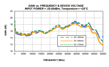
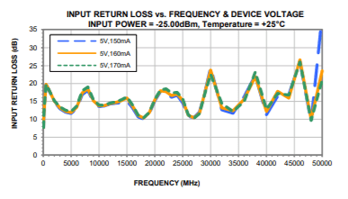
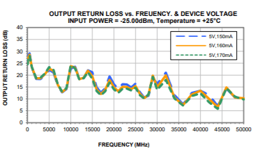
Mini-Circuits has invested in adding distributed amplifiers to its MMIC portfolio to support customer needs. One of the latest distributed amplifier models released is the LTA-M1109-D+. This model has a wide operating bandwidth of DC to 50 GHz with 17 dB gain and ±2.2 dB flatness. It has good P1dB of 20.7 dBm at 0.1 GHz and 17.9 dBm at 30 GHz. Performance curves for gain, input return loss and output return loss are shown below in Figure 5.
Figure 5: Left to right, gain, input return loss and output return loss of Mini-Circuits’ LTA-M1109-D+ distributed MMIC amplifier.
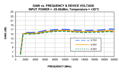
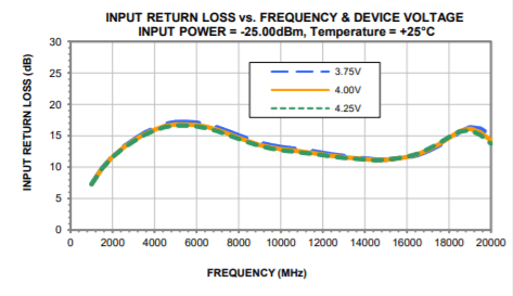
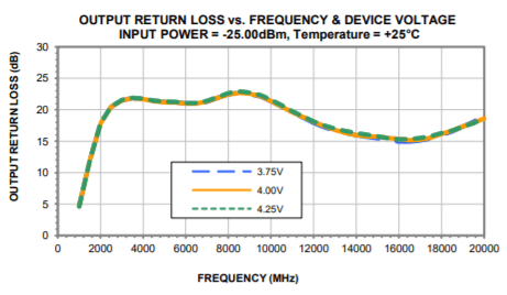
Another of our recent distributed amplifier models is the LTA-2183-D+. This amplifier operates from 2 to 18 GHz with 16 dB gain and ±0.7 dB flatness over its full frequency range. It provides 19.6 dBm typical output power at 1 dB compression, 27.6 dBm OIP3 and 47.4 dB directivity. The amplifier operates on a 4V supply with 210 mA DC current consumption. Performance plots for gain, input and output return loss are shown below in Figure 6.
Figure 6: Left to right, gain, input return loss and output return loss of Mini-Circuits’ LTA-2183-D+ distributed MMIC amplifier.
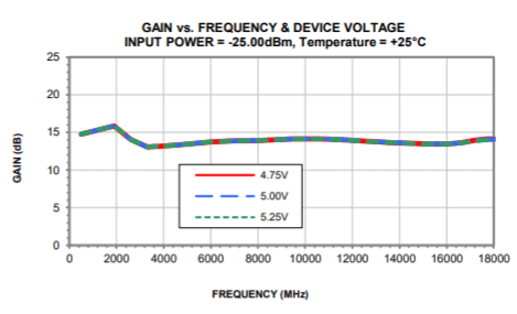
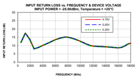
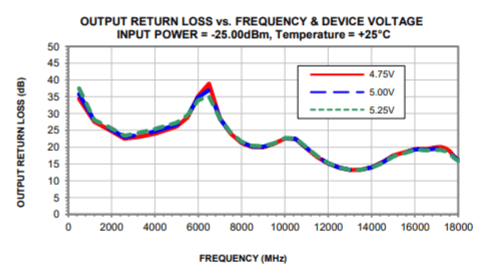
Another example of a Mini-Circuits distributed amplifier is LTA-5R183-D+. This is amplifier covers an even wider frequency range, extending from 500 MHz to 18 GHz. It delivers 18.6 dBm P1dB with a gain of 13 ±1.6 dB, and a noise figure around 3 dB. Figure 7 shows performance plots for the gain, input and output return loss for this amplifier.
Figure 7: Left to right, gain, input return loss and output return loss of Mini-Circuits’ LTA-5R183-D+ distributed MMIC amplifier.
Additional models employing distributed amplifier designs are currently in development to support ultra-wide bandwidths well into the millimeter wave (mmWave) range.
Summary
Distributed architectures enable amplifiers with good performance over exceptionally wide bandwidths. This capability is especially useful for the growing range of wideband systems extending higher up the frequency spectrum. Mini-Circuits has invested in the technology and the engineering talent to develop distributed amplifiers, some of which are already available from stock with others in development and coming soon.


