

Best Practices for Additive Phase Noise Measurements in Amplifiers
Shradha Basil, Mini-Circuits Applications
In a previous article titled “Additive Phase Noise in Amplifiers,” we covered: the basic definitions of additive phase noise, the reasons it’s such an important parameter for many communication systems, and newly available specs for several of Mini-Circuits’ MMIC amplifier models. Since then, several customers interested in these products have asked for details about Mini-Circuits’ additive phase noise measurement setup. Such questions are only natural, considering additive phase noise is a notoriously mercurial parameter to measure. It’s important to know the published performance data is reliable and accurate, and to understand the operating conditions under which measurements were taken when evaluating parts for your design.
This article will review the challenges in measuring additive phase noise and present details of the measurement setup Mini-Circuits uses to perform these measurements accurately and reliably. We will also dive into the specifics of additive phase noise readings and explain how to interpret phase noise values and measurement plots.
Measurement Challenges
One of the biggest challenges in accurately measuring additive phase noise is making sure the DUT and only the DUT is being measured. Several factors can introduce external noise into the measurement setup, and it is critical to minimize these effects. In a lab environment, everything from the signal source to the DC power supply to the amplifier and even environmental factors like temperature, vibration and ambient EMI can have significant impacts on the integrity of the measurement. In the next few sections, we will look into how Mini-Circuits’ measurement setup minimizes external noise sources to achieve accurate results.
Another challenge is ensuring repeatability from measurement to measurement over different carrier frequencies and signal power levels. It is essential to go back and repeat certain measurement points if any anomalies exist after observing the preliminary data. Such anomalies, if present, are often associated with the power delivered to the internal phase detector being either too high or too low. It is not unusual for ±1 dB changes in power to improve or degrade the results. Similarly, depending upon the DUT voltage and current requirements, it is not unusual for the power supply to introduce noise into the measurement. Additional R-L-C filtering, for example, may be needed on the DC input to help suppress this parasitic noise. Mini-Circuits’ additive phase noise measurement setup was designed to account for all these challenges to ensure consistency from measurement to measurement.
Additive Phase Noise Measurement Setup
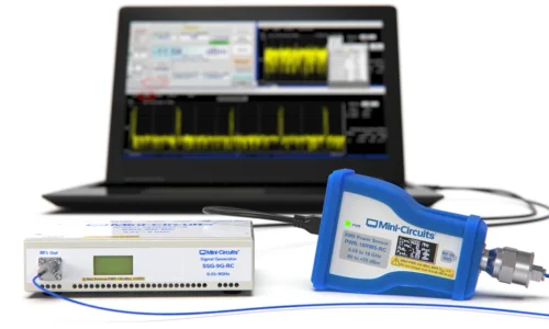
Selecting the right test equipment is perhaps the most critical part of a reliable test setup. Mini-Circuits evaluated several different options and ultimately selected the model with the best additive performance in the offset region from roughly 10 kHz to 300 kHz. This allowed us to highlight the extraordinary performance of the majority of our HBT-based amplifiers. The selected model also has an upper frequency measurement limit of 8 GHz. This compromise was made because for frequencies above 8 GHz, the test equipment system noise floor is often greater than the additive phase noise of the DUT.
Also critically important is creating a test setup that ensures accuracy and repeatability. Figure 1 shows the functional block diagram and signal flow for the compete test setup used for additive phase noise measurement:

The phase noise analyzer acts as both signal generator (Tx) and analyzer (Rx). This setup uses a combination of variable and fixed attenuators. A variable attenuator is used at the analyzer’s signal source output to vary the input power to the DUT, and another fixed attenuator directly at the input of the DUT is used to improve matching. The mechanical attenuator at the analyzer’s input is crucial, as it not only helps to ensure the maximum input power to the analyzer is never exceeded, but also gives the test operator the freedom to vary the power level into the analyzer to the optimum level for the best phase noise readings. It also ensures that the phase detector is always being operated within a narrow range of input powers. This further improves repeatability.
Most of the additional components in this setup are passive to ensure a “noiseless” way to vary and measure signal power. Coupler 1 is used to monitor the input power to the DUT (amplifier) and also to ensure its maximum input power rating isn’t exceeded. Coupler 2 samples the output power of the amplifier, which is also used to determine the amplifiers’ region of operation (i.e. linear or saturation). Power sensors are connected to the coupled ports of both couplers and then to the analyzer via USB, which enables the operator to read power levels directly on the measurement screen (Figure 3). These sensors are sufficiently decoupled from the main transmission paths so that any spurious contributions are essentially negligible and do not influence the accuracy of the additive phase noise measurements.
The analyzer has an internal power sensor that is used to measure the power at the phase detector input. This power level is adjusted using the mechanical step attenuator mentioned earlier. It is important to state that there are actually three power levels being adjusted and monitored: The DUT input power, DUT output power and the phase detector input power.
The entire test setup, including the phase noise analyzer and the peripheral components are placed in an EMI shielded enclosure to prevent interference from external signals. The test equipment and test apparatus inside the EMI enclosure is then placed on vibration damping material. The entire setup is placed on a sturdy table to provide mechanical stability and minimize any effects of movement during the measurement process.

We know that the DC power supply can be a significant contributor to phase noise, and we experimented with different power supplies and shielding methods to find one that adds minimal noise to the system and, again, ensure we’re measuring the performance of the DUT and not contributions of external factors. Before testing the DUT, the losses of all the other components in the setup are measured at the intended carrier frequency and calibrated out.
Understanding Additive Phase Noise Measurements
In studying the details of phase noise readings, it is important to understand what phase noise looks like in theory. The additive phase noise of an amplifier is represented on a graph with frequency offset on the X-axis and normalized carrier power in a 1 Hz bandwidth in dBc/Hz on the Y-axis. Ideally, the frequency response should be a single tone at the carrier frequency. In reality, with phase noise, we see the response spread out around the carrier, often described as a “skirt” shape (Figure 3).
We would expect all the power to be concentrated at the carrier or near it, but the presence of phase noise distributes power at various ranges away from the carrier as well. It is therefore important to quantize signal power as a function of distance from the carrier. This is done by measuring the values of signal power with respect to the carrier (dBc) at different frequency offsets away from the carrier. To characterize phase noise, it is enough to look at only the single sideband, since AM and PM are symmetrical about the carrier frequency.

The unit used to represent phase noise is dBc/Hz and represents the ratio of carrier power to the power measured in a 1 Hz bandwidth at a specific frequency offset from the carrier frequency. Therefore, when describing phase noise performance of any DUT, it is important to mention the phase noise value itself in dBc/Hz, but also the carrier frequency and the offset at which we measured this value. Figure 4 shows an example measurement on the measurement screen of the phase noise analyzer.

This measurement was performed at a carrier frequency of 2 GHz, and signal level indicates the input power at the internal phase shifter. This value is optimized using the external variable attenuators to achieve the best possible phase noise readings. Resolution bandwidth and cross-correlation (XCORR) factors are parameters that are adjusted to improve the accuracy of the measurement and have a direct impact on measurement time.
In Figure 4, the yellow trace represents PM noise and the blue trace indicates AM noise. Each marker indicates phase noise values at different frequency offsets from the carrier frequency of 2 GHz. For example, at 1 kHz offset, the phase noise is -163.14 dBc/Hz and at 1 MHz offset, the phase noise is -172.02 dBc/Hz. Increasing offsets means we are moving further away from the carrier. It is obviously desirable to have low signal power with respect to the carrier the further out from the carrier we go. The lower the phase noise, the better the overall system performance
Measurement Results
As a part of our evaluation of the analyzer and characterization of additive phase noise for our amplifiers, data for which was shared in the previous article, we also performed additional testing to understand the factors that affect additive phase noise performance of the amplifier itself. In the previous sections we discussed how we create a reliable setup. But further to understanding how the measurement is performed, it’s important for users to understand all the different variables upon which additive phase noise performance depends.
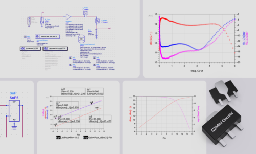
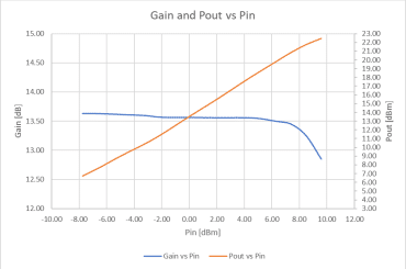
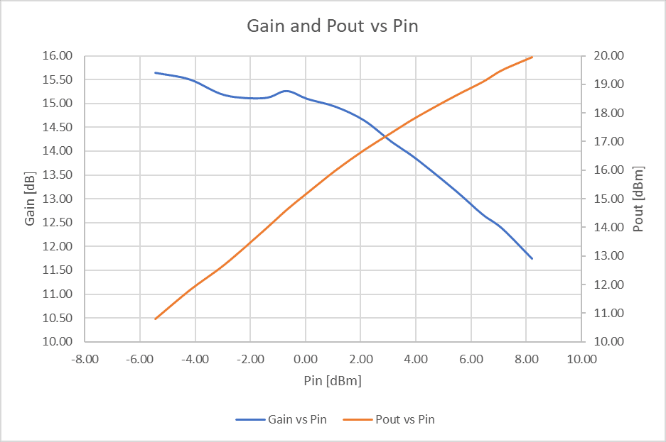
We will now look into inherent additive phase noise performance variations over different input powers, operating regions (linear/saturation) and carrier frequencies. Figure 5 shows a performance comparison of two different MMIC amplifiers over different input powers. Both models are 0.5µm InGaAs E/D mode designs. The variation in performance as a function of input power is immediately evident. The Gain and Pout vs Pin curves provide a reference to show how additive phase noise performance changes over the operating region of the amplifier. These measurements were performed at a carrier frequency of 2 GHz.
Figure 5: Comparison of additive phase noise performance for two different 0.5µm InGaAs E/D Mode MMIC amplifiers.
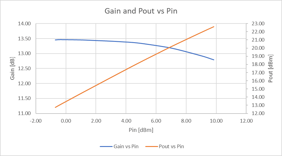
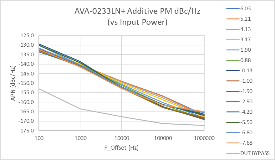
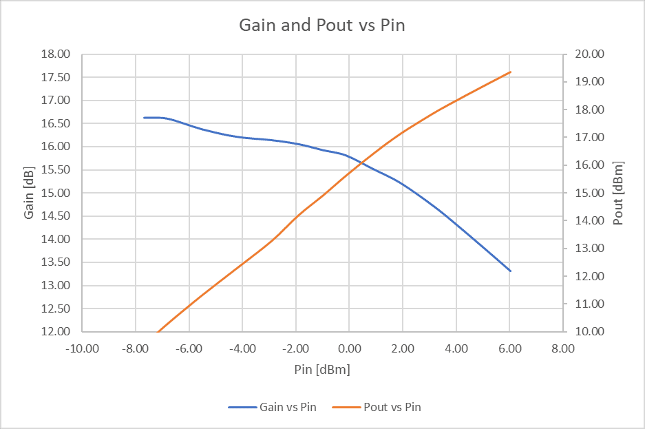
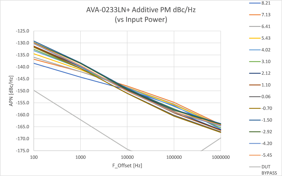
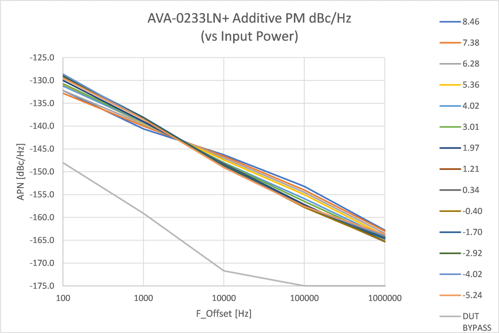
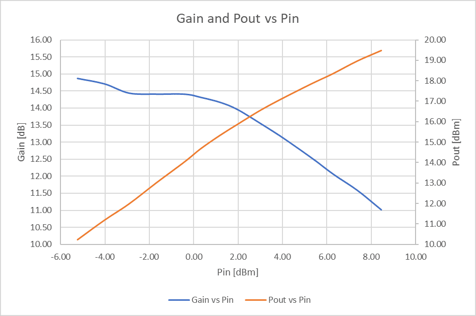
Aside from variation over input power, additive phase noise may change over different carrier frequencies. Plots below illustrate phase noise performance of the 0.25µm GaAs pHEMT amplifier AVA-0233LN+ at three different carrier frequencies. Gain and Pout vs. Pin are shown again as to indicate the amplifiers’ operating region at different input power levels.
Carrier Frequency: 2000 MHz
Carrier Frequency: 4000 MHz
Carrier Frequency: 6000 MHz
Figure 6: Additive phase noise performance of 0.25µm GaAs pHEMT amplifier AVA-0233LN+ at three different carrier frequencies.
Evaluating additive phase noise performance under different conditions can be of great help to customers in understanding the usefulness of an amplifier in certain applications. For example from the above plots we can see that the AVA-0233LN-D+ may be run under saturated output power conditions without degrading additive phase noise, and this makes it suitable for LO driver applications.
The appendix includes plots that show variation of additive phase noise values over input power at individual offsets. There is no universal best operating point for all amplifiers for all offsets. The customer’s unique application requirements are the key to identifying the best operating point and selecting the right amplifier.
Summary
In this article we reviewed the challenges of measuring additive phase noise in amplifiers. We presented the phase noise measurement setup Mini-Circuits uses to test additive phase noise in amplifiers and explained the different features of the setup in detail. Lastly, we explained how to interpret phase noise measurements with respect to carrier frequency, frequency offset and signal power. Mini-Circuits also characterizes AM noise, which will be discussed in a subsequent article.
Ultimately, this explanation is meant to give you confidence in the accuracy of the information Mini-Circuits provides about the phase noise performance of its amplifiers. Whether you’re working with Mini-Circuits or other suppliers, if phase noise is an important consideration in your amplifier selection, we urge you to scrutinize the measurement methods used to ensure the information is accurate and consistent. Diligence upfront will avoid unexpected results and additional design time when you integrate the amplifier into your system.
For additional questions about phase noise in Mini-Circuits amplifiers, please reach out to our application engineers to speak with one of our engineers.
Appendix
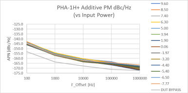
PHA-1H+ @ Carrier Frequency 2 GHz

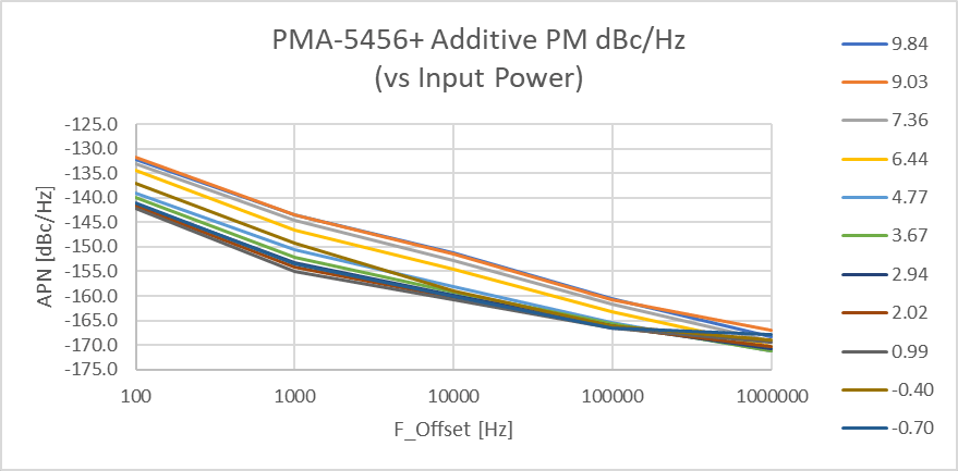
PGA-105+ @ Carrier frequency 2 GHz

AM Noise measurements (Fc=2 GHz)


