MCDI - Mini-Circuits Exclusive Representative in Israel

Impedance Matching Devices

Stephen Leone and William Yu, Mini-Circuits Applications

Introduction to Impedance Matching

The impedance of a component or transmission line is a major concern when designing RF/microwave systems.  At the circuit level, optimum performance is obtained when devices are matched to the desired system impedance, typically 50Ω or 75Ω. At the system level, each building block must be matched to the system impedance to maintain performance along the signal path.

Without matching, there can be abrupt changes – or mismatches – of impedance along a signal’s path. Anytime there is a mismatch in a system, a portion of the signal power is reflected instead of being transferred efficiently to the load. Larger impedance mismatches correspond with larger reflections. This results in increased loss in the forward signal, as well as distortion caused by interaction between the signal and the reflection. Moreover, as the reflected signals propagate throughout the system, they can cause interference which degrades overall system performance. Matching quality is measured as return loss, which is the essentially the difference in magnitude between the incoming signal and the reflection. Thus, optimal performance is obtained with a high value of return loss.

The most common impedance for RF systems is 50Ω. 75Ω is also common, mainly for applications such as Cable TV and radio or TV antennas. In some cases, a system may include both 50Ω and 75Ω devices, requiring an impedance matching device to reduce the reflected power and avoid signal degradation.

Matching Techniques

Impedance matching devices can be separated into two categories: those that are lossy, implemented with resistive components; and those that are ideally lossless, using reactive components—inductors, capacitors, and transmission lines.

The main advantage of lossy impedance matching devices is that they provide good return loss over a wide bandwidth. They also have a simple design. Because they are usually implemented with just resistive components, lossy devices will almost always operate down to DC.

Lossless impedance matching devices use reactive elements to maximize power transfer. They are also capable of matching a reactive source or load impedance (R ± jX) to a resistive system impedance. Because reactances are frequency-dependent, the performance of these devices will be optimized either at a single design frequency or within a given bandwidth.

Lossy Devices

Matching Pads

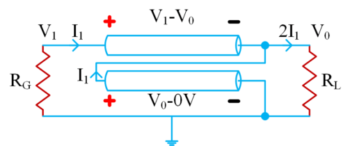
The most common lossy impedance matching device is the L-pad, also known as the minimum loss pad. This is simply composed of a series and a shunt resistor. As its name suggests, the minimum loss pad is the configuration that results in the lowest insertion loss while still matching impedances from both directions. Below is the schematic for an L-pad. Assuming ZA>ZB, the following equations can be derived using Ohm’s Law. (1) represents the impedance as seen by ZA, and (2) represents the impedance seen by ZB. In order to properly match ZA to ZB, each must see an impedance equal to itself.

Figure 1: Schematic for an L-Pad
Impedance Matching Devices

Solving for R1 and R2, we get:

Impedance Matching Devices

For ZA = 75Ω and ZB = 50Ω, R1 = 86.6Ω and R2 = 43.3Ω, resulting in a minimum loss of 5.7 dB. Note that the minimum achievable loss increases as the difference between the two impedances being matched increases.

Matching pads are the simplest matching devices to design and will operate from DC to high frequencies. However, they are not the most power inefficient, with an unavoidable minimum insertion loss.

Lossless Devices

Step Transition

The naïve approach to impedance matching is to not do any matching at all. The step transition is what you get by directly transitioning from one impedance to another while accepting the worst-case reflection. This non-device is ideally lossless but will not transmit the full power due to the mismatch. For a 50Ω to 75Ω step transition, 4% of the input power is reflected and the remaining 96% is transmitted. This may not seem like a significant loss of transmitted power, but that amount of reflected power can cause real problems in many systems.

Core and Wire Transformers

A typical core and wire transformer transfers power between two coils of wire wrapped around a ferromagnetic core. Ideal transformers are able to change the voltage-to-current ratio, or impedance, of a signal without dissipating any power. However, a real transformer will have inevitable losses which are mostly due to imperfections in the core material and magnetic flux leakage. Mini-Circuits transformers approach ideal performance by using high-permittivity materials and precision manufacturing tolerances to achieve tight coupling between coils over a wide bandwidth.

The impedance ratio between the primary and secondary sides of a transformer is determined by the ratio of the number of turns on the secondary side (n2) to the number of turns on the primary side (n1).  The impedance ratio can be calculated as the square of the turns ratio.

Impedance Matching Devices

For a 50Ω : 75Ω transformer, the impedance ratio is 1:1.5 and the turns ratio is 1:1.22 which can be implemented by 4.5 turns on the primary (50Ω) side and 5.5 turns on the secondary (75Ω) side.

Because they utilize the permeability of a magnetic core, traditional transformers are able to operate down to very low frequencies and over wide bandwidth in a very small form factor. Parasitic effects, such as interwinding capacitance, increase with frequency, which limits the upper frequency range of operation.

Quarter Wave Transformers

Quarter wave transformers are the transmission line approach to the matching problem. A lossless transmission line with characteristic impedance Z0, length l, and a load impedance ZL, will observe an impedance of Zin according to the following equation:

Impedance Matching Devices

To implement a quarter wave transformer to match to impedances Zin and ZL, the system designer need simply place a series transmission line that is ¼ λ long at the operating frequency, with a characteristic impedance of  Zo=Sqrt(ZinZL) between the two impedances. Because these transformers are simply transmission lines, they have the benefits of passing DC current and handling high RF power levels. Coupled with the fact that these devices have very efficient power transfer, transmission line transformers are extremely useful were the signal power is high and the insertion loss is critical such as between a power amplifier and a transmit antenna.

The primary disadvantage is that quarter wave transformers can only provide good matching over about an octave bandwidth around the center frequency.

Figure 2: Schematic of a Quarter Wave Transformer

L-C Networks

As the name implies, L-C matching networks consist of only reactive components: inductors (L) and capacitors (C). Similar to the L-pad, the simplest matching network consists of one series and one shunt component.

Below are schematics of an L-C network. X1 can be either an inductor or capacitor, while X2 is the other of the two components. R1 and R2 represent real impedances that are to be matched, where R1 > R2.

Impedance Matching Devices
Figure 3: Schematics of an L-C Network

The impedance of R1 in parallel with X1 equates to

Impedance Matching Devices

This is also equivalent to

Impedance Matching Devices

In order to match R2 to R1, the series X2 component needs to cancel with the complex impedance of R1 in parallel with X1, while X1 needs to be chosen such that R2 matches the real impedance of R1 in parallel with X1.

This gives us the following equations:

Impedance Matching Devices

Solving for X1 and X2, we get:

Impedance Matching Devices

and where positive X1, X2 refers to inductive reactance, and negative X1, X2 refers to capacitive reactance.

The advantages of L-C matching networks are that they use inexpensive components, have low loss, and provide wideband matching at lower frequencies. However, since they use lumped elements, they are limited at higher frequencies where transmission line effects become significant. Furthermore, they are more difficult to design than matching pads, and are limited by component sizes when used for large mismatches.

Key Parameters

Impedance matching devices are characterized with the following parameters:

  • Insertion loss — Power loss of the device under matched conditions.
  • Max RF Input Power — The maximum RF power that can be handled without risking permanent damage to the device.
  • Bandwidth — The frequency range where the electrical specifications are applicable.
  • Impedance ratio — The impedance ratio defines what impedances the device will be used to match. For transformers, this refers to the ratio of the secondary impedance to the primary impedance.
  • Return Loss/VSWR — Defines the magnitude of the reflected power from the input or output ports, assuming perfect loads.

How to choose a matching device

There are numerous factors to consider when choosing an impedance matching device for a given application. The process can generally be broken down into a few primary steps to narrow down the options and identify the ideal solution.

Step 1: What are the impedances to be matched?
A clear definition of the impedances that need matching allows us to know what technologies are viable for the desired impedance match.

Step 2: Surface mount or connectorized case style?
This choice will determine the available technologies and models in our catalog. Not all Mini-Circuits’ surface mount components have connectorized equivalents, and transmission line transformers do not have surface mount equivalents.

Step 3: Are there any requirements for DC isolation or DC continuity?
Typically, all transmission line matching devices will pass DC. L-C networks and transformers may or may not have DC isolation or continuity, depending on the design.

Step 4: What are the RF electrical requirements?
Determine the performance specifications for the desired application. The previous sections describe the electrical parameters relevant to impedance matching devices. Filtering models by performance parameters will further narrow the pool of suitable options.

Mini-Circuits Impedance Matching Devices

Mini-Circuits’ connectorized impedance matching devices are most useful for test applications and lab use or for implementing 75Ω systems. 50Ω is the industry standard for most RF devices. However, 75Ω is still widely used for CATV and satellite receiver applications. When a system designer wants to use a 50Ω connectorized device in a 75Ω system or vice versa, impedance matching is strongly recommended. In addition to improving system performance from an electrical standpoint, connectorized devices offer the mechanical advantage of interfacing a 75Ω connector with a 50Ω connector. In many cases, these devices are the only option for this interface. Mini-Circuits provides lossy and lossless impedance matching options for a wide variety of standard connectors. In this section we will highlight some products which use the technologies discussed in the previous sections.

The SFQFM-5075+ is a connectorized resistive matching pad designed for optimal return loss from DC-3000 MHz. The measured data shown in Figure 4 shows better than 25 dB return loss, and the expected 5.7 dB insertion loss. The SFQFM-5075+ features an SMA-female and a quick-connect F-type male connector. Quick connect connectors are designed with fewer threads so that they can be tightened in a single rotation. This is especially useful for achieving higher throughput in production test setups for 75Ω connectorized modules.

Impedance Matching Devices
Figure 4: Left: SFQFM-5075+ connectorized 50Ω SMA to 75Ω F-type matching pad. The quick-connect F-type connector has a reduced number of threads compared to a traditional F-type. Right: SFQFM-5075+ RF performance.
Impedance Matching Devices

The Z7550-FMSF+ and SFMP-5075+ are low-loss connectorized impedance matching devices. The Z7550-FMSF+ is a transmission line transformer with a 1250 MHz center frequency. This allows good matching over a relatively narrow bandwidth and excellent insertion loss up to 2500 MHz. Mini-Circuits’ transmission line transformers have the best power handling of all our matching devices. These devices have survived 24-hour burn-in tests at 25W input power, while showing no noticeable degradation in performance. In addition, they are ideal for feeding high DC currents to the output of a power amplifier which is mismatched to the system impedance.

The SFMP-5075+ is a 4-pole L-C transformation network. Given that the device consists of only reactive components, it has comparable performance to the Z7550-FMSF+. The lumped element design allows for a smaller form factor than the Z7550-FMSF+ transmission line design. The contrast is especially pronounced at lower design frequencies.

Impedance Matching Devices
Figure 5: Top Left: Z7550-FMSF+ Connectorized 50Ω SMA to 75Ω F-Type Transmission Line Transformer. Bottom Left: SFMP-5075+ Connectorized 50Ω SMA to 75Ω F-Type LC Matching Network. Right: Low Loss Matching Transformer Comparison. Z7550-FMSF+ (Transmission Line) and SFMP-5075+ (LC Network).

The FT-1.5-232-SF+ is a connectorized core and wire transformer. The FT-1.5-232-SF+ is ideal for designs where optimal matching is required below 1500 MHz. From the technologies we have discussed. The core and wire matching transformers are a good balance between transmission and reflection performance and are the only option for near-lossless matching at very low frequencies.

Impedance Matching Devices
Figure 6: FT-1.5-232-SF+ Connectorized 50Ω SMA to 75Ω F-Type Core and Wire Transformer
Impedance Matching Devices

In addition to SMA to F-Type connectorized devices, Mini-Circuits offers connectorized impedance matching for several standard 50Ω and 75Ω connector options (see Table 1). Combined with our comprehensive selection of adapters, it is easier than ever to convert from any one connector type to any other with minimal reflections.

Impedance Matching Devices
Table 1. Connectorized matching transformers available in the Mini-Circuits catalog by connector 50Ω and 75Ω connector type and technology

Matched vs Unmatched System

We have discussed the importance of reducing reflections in RF systems at length, but up to this point, we have only considered the case of a single mismatch. In any realistic RF system, every device transition will present a discontinuity, all of which will be separated by line lengths. If a portion of a signal is reflected by one discontinuity, that reflection will travel in the reverse direction. If it is then re-reflected by a second discontinuity, it will travel in the same direction as the original signal. At the very least, signals that are re-reflected from two or more discontinuities combine coherently and non-coherently to generate ripples in the insertion loss over the frequency range. The period of these ripples is inversely proportional to the length of the line, and the amplitude is proportional to the amount of signal reflected by the discontinuities. Transmission ripples are undesirable because a high instantaneous slope in the insertion loss causes distortions in wideband signals. For calibrated systems, small shifts in cable position can cause large inaccuracies if there is a large amount of ripple. Ideally, we would like to remove the ripple without introducing too much loss. As shown in Figure 7 below, adding the FT-1.5-232-SF+ ti the system trades off the ripple for a small linear slope in the insertion loss. Such gain slopes are routinely compensated out using slope equalization and calibration techniques.

Impedance Matching Devices
Figure 7. Left: Schematic of 75Ω cable in a 50Ω system with no matching device (step transition) above and with core and wire matching transformers below. Right: Insertion loss ripple caused by step transitions and impedance matching using the FT-1.5-232-SF+

Conclusion

Impedance matching is one of the key factors in RF and microwave design.  Proper impedance matching achieves efficient power transfer and minimizes unwanted reflected signals. Those reflections can result in excessive loss, self-interference, instability, and a reduction in the accuracy and integrity of modulated signals.

Mini-Circuits offers a wide variety of impedance matching products covering the range of frequencies most needed for today’s applications. These products offer several matching techniques to provide design solutions with low loss, accurate impedance transformation and wide bandwidth, which allows our customers to select the optimal device for their RF systems.

View all Impedance Matching Pads

Liked this article? Please share it!

One last thing...

Aharon

Before you leave, you should know that MCDI’s professional team of Application Engineers  will be delighted to assist you in sourcing the right component. Just fill the form and we will be back to you shortly.